Proceedings of the National Academy of Sciences of the United States of America

Edited by J. B. Pendry, Imperial College London, London, UK, and approved December 17, 2020 (received for review June 21, 2020)
Author contributions: A.T.C., P.A.D.G., N.A.M., and N.M.R.P. designed research; A.T.C., P.A.D.G., F.H.L.K., N.A.M., and N.M.R.P. performed research; A.T.C., P.A.D.G., D.N.B., F.H.L.K., N.A.M., and N.M.R.P. analyzed data; and A.T.C., P.A.D.G., D.N.B., F.H.L.K., N.A.M., and N.M.R.P. wrote the paper.
- Altmetric
Superconductivity and plasmonics constitute two extremely vibrant research topics, although with often nonoverlapping research communities. Here, we bridge these two active research fields by showing that graphene plasmons’ unprecedented light localization into nanometric scales can be exploited to probe the electrodynamics (including collective excitations) of superconductors. Our findings are important both from a fundamental standpoint, representing a paradigm shift (i.e., probing of Higgs modes by light fields), and also for future explorations interfacing nanophotonics with strongly correlated matter, which holds prospects for fostering additional concepts in emerging quantum technologies.
We show that the Higgs mode of a superconductor, which is usually challenging to observe by far-field optics, can be made clearly visible using near-field optics by harnessing ultraconfined graphene plasmons. As near-field sources we investigate two examples: graphene plasmons and quantum emitters. In both cases the coupling to the Higgs mode is clearly visible. In the case of the graphene plasmons, the coupling is signaled by a clear anticrossing stemming from the interaction of graphene plasmons with the Higgs mode of the superconductor. In the case of the quantum emitters, the Higgs mode is observable through the Purcell effect. When combining the superconductor, graphene, and the quantum emitters, a number of experimental knobs become available for unveiling and studying the electrodynamics of superconductors.
The superconducting state is characterized by a spontaneously broken continuous symmetry (1). As a consequence of the Nambu–Goldstone theorem, superconductors are expected to display two kinds of elementary excitations: the so-called Nambu–Goldstone (NG) and Higgs modes (23–4). The NG mode is associated with fluctuations of the phase of the order parameter, whereas the Higgs mode is related to amplitude fluctuations of the same. In superconductors and electrically charged plasmas, the NG (phase) mode couples to the electromagnetic field and its spectrum effectively acquires a gap (mass) due to the long-range Coulomb interaction (Anderson–Higgs mechanism) (2); this gap corresponds to the system’s plasma frequency (1, 5, 6). On the other hand, the Higgs (amplitude) mode is always gapped, and in superconductors its minimum energy is equal to twice the superconducting gap (7). Curiously, one often encounters in the literature statements that the Higgs mode does not couple to electromagnetic fields in linear response, making it difficult to observe in optical experiments (2, 8). Experimental detection has been achieved only through higher-order response, e.g., by pumping the superconductor with intense terahertz fields and measuring the resulting oscillations in the superfluid density (9101112–13). [It has been recently suggested, however, that the observed oscillations could be interpreted as resulting from excitation of the NG mode instead (8, 141516–17). Additionally, it has also been pointed out that the Higgs mode may be observed in disordered superconductors (18), as long as one chooses to measure the appropriate response function (19).]
Naturally, the light–Higgs coupling is subjected to conservation laws, whereby translational invariance manifests in the conservation of wave vectors. Since far-field photons carry little momentum, wave vector conservation cannot be satisfied and the coupling is suppressed. However, little attention has been given to the fact that, strictly speaking, the linear-response coupling of the electromagnetic field to the Higgs mode effectively vanishes only in the limit (8, 20). As such, at finite wave vectors—i.e., in the nonlocal regime—the linear optical conductivity of the superconductor yields a finite contribution associated with the coupling to the Higgs mode (8, 20, 21). Hence, electromagnetic near fields provided by, for instance, plasmons, emitters, or small scatterers can couple to such amplitude fluctuations and therefore constitute a feasible, promising avenue toward experimental observations of the Higgs mode in superconductors. In this context, ultraconfined graphene plasmons (22, 23) constitute an additional paradigm for probing quantum nonlocal phenomena in nearby metals (2324252627–28), while their potential as tools for studying the intriguing electrodynamics of strongly correlated matter (2930–31) remains largely virgin territory.
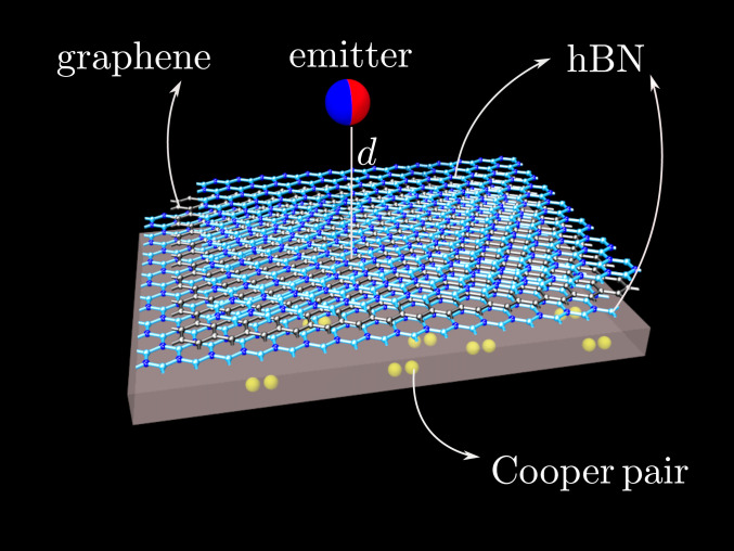
Here, we exploit the unprecedented field confinement yielded by graphene plasmons (GPs) (23, 252627–28 32) for investigating the near-field electromagnetic response of a heterostructure composed of a graphene sheet separated from a superconductor by a thin dielectric slab (Fig. 1). Both the superconductor and the graphene sheet are characterized by their optical conductivity tensors (21, 22). The optical conductivity tensor of the superconductor is intrinsically nonlocal (21), whereas for graphene it is possible to employ a local-response approximation at wave vectors much smaller than graphene’s Fermi wave vector (22, 25, 26). We show that the coupling between the Higgs mode in the superconductor and plasmons in the graphene manifests itself through the existence of an anticrossing-like feature in the near-field reflection coefficient. Furthermore, the energy and wave vector associated with this feature can be continuously tuned using multiple knobs, e.g., by changing 1) the temperature of the superconductor, 2) the Fermi level of the graphene sheet, or 3) the graphene–superconductor separation.


Schematic of the graphene–superconductor hybrid device considered here. Shown is an illustration of the heterostructure composed of a superconducting substrate, a few atomic layers of hexagonal boron nitride (hBN), a single sheet of graphene, and a capping layer of hBN. It should be noted that although here the hBN has been depicted in monolayer form, our model can accommodate any number of hBN layers. The red-blue sphere represents an electric dipole placed above the heterostructure.
Finally, we suggest an alternative observation of the GPs–Higgs coupling through the measurement of the Purcell enhancement (23, 33, 34) near the heterostructure. To that end, we calculate the electromagnetic local density of states (LDOS) above the graphene–dielectric–superconductor heterostructure; our results show that, in the absence of graphene, the coupling between the superconductor’s surface polariton and its Higgs mode leads to an enhancement of the LDOS near the frequency of the latter. The presence of graphene changes qualitatively the behavior of the decay rate around the frequency of the Higgs mode, depending strongly on the emitter–graphene distance.
Theoretical Background
Electrodynamics of Bardeen–Cooper–Schrieffer-Like Superconductors.
The electrodynamics of superconductors and other strongly correlated matter constitute a fertile research area (29, 30). In the following, we assume that the superconducting material is well described by the Bardeen–Cooper–Schrieffer (BCS) theory of superconductivity (21, 35, 36). Chiefly, the microscopically derived linear optical conductivity tensor of a superconductor requires a nonlocal framework due to the finiteness of the Cooper-pair wave function. For homogeneous superconducting media, the longitudinal and transverse components of the nonlocal optical conductivity tensor—while treating nonlocality to leading order—can be expressed as (21, 37, 38)*
In possession of the response functions epitomized by Eq. 1, we employ the semiclassical infinite barrier (SCIB) formalism (23, 39) to describe electromagnetic phenomena at a planar dielectric–superconductor interface (37, 38, 40). Within this framework, the corresponding reflection coefficient for
In what follows, we assume a typical high-
Electrodynamics in Graphene–Dielectric–Superconductor Heterostructures.
With knowledge of the reflection coefficient for the dielectric–superconductor interface (2), the overall reflection coefficient, i.e., that associated with the dielectric–graphene–dielectric–superconductor heterostructure, follows from imposing Maxwell’s boundary conditions (42) at all of the interfaces that make up the layered system. At the interface defined by the two-dimensional graphene sheet, the presence of graphene enters via a surface current with a corresponding surface conductivity (22).
Signatures of the system’s collective excitations can then be found by analyzing the poles of the corresponding reflection coefficient, which are identifiable as features in the imaginary part of the (overall) reflection coefficient,
Coupling of the Higgs Mode of a Superconductor with Graphene Plasmons
Signatures of the Higgs Mode Probed by Graphene Plasmons.
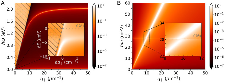
Like ordinary conductors (44), superconductors can also sustain surface plasmon polaritons (SPPs) (45, 46). In turn, these collective excitations can couple to the superconductor’s Higgs mode (37, 38). Typically such interaction is extremely weak due to the large mismatch between the superconductor’s plasma frequency,


Spectra of surface electromagnetic waves in superconductors (A) and graphene–superconductor (B) structures, obtained from the calculation of the corresponding
On the other hand, graphene plasmons not only span the terahertz regime but also attain sizable plasmon wave vectors at those frequencies (22, 23). Moreover, when the graphene sheet is near a metal—or a superconductor for that matter—graphene’s plasmons become screened and acquire a nearly linear (acoustic) dispersion, pushing their spectrum further toward lower frequencies (i.e., a few terahertz) and larger wave vectors (23242526–27, 32). Therefore, these properties of acoustic-like GPs can be harnessed by placing a graphene monolayer near a superconducting surface, thereby allowing the interaction of graphene’s plasmons with the Higgs mode of the underlying superconductor (Fig. 2B). In this case the plasmon–Higgs interaction is substantially enhanced, a fact that is reflected in the observation of a clear anticrossing in the GP’s dispersion near
Furthermore, the use of graphene plasmons for probing the superconductor’s Higgs mode comes with the added benefit of control over the plasmon–Higgs coupling by tuning graphene’s Fermi energy electrostatically (22, 23, 4748–49). This is explicitly shown in Fig. 3A, for a vacuum–hexagonal boron nitride (hBN)–graphene–hBN–superconductor heterostructure; as before, the coupling of GPs with the superconductor’s Higgs mode manifests itself through the appearance of an avoided crossing in the vicinity of

![Tuning the hybridization of acoustic-like plasmons in graphene with the Higgs mode of a superconductor in air–hBN–graphene–hBN–superconductor heterostructures. The colormap indicates the loss function via Im rp. (A and B) Spectral dependence upon varying the Fermi energy of graphene (A) and the graphene–superconductor distance (B). Setup parameters: The parameters of the superconductor are the same as in Fig. 2, and the same goes for graphene’s Drude damping. The thickness of the bottom hBN slab is given by t, whereas the thickness of the top hBN slab, t′, has been kept constant (t′=10 nm). Here, we have modeled hBN’s optical properties using a dielectric tensor of the form ϵ↔hBN=diag[ϵxx,ϵyy,ϵzz] with ϵxx=ϵyy=6.7 and ϵzz=3.6 (24, 49, 50).](/dataresources/secured/content-1765838872807-4c08a48c-9f30-4889-8612-bdc806605179/assets/pnas.2012847118fig03.jpg)
Tuning the hybridization of acoustic-like plasmons in graphene with the Higgs mode of a superconductor in air–hBN–graphene–hBN–superconductor heterostructures. The colormap indicates the loss function via
Higgs Mode Visibility through the Purcell Effect.
One way to overcome the momentum mismatch and investigate the presence of electromagnetic surface modes is to place a quantum emitter (22, 5152–53) (herein modeled as a point-like electric dipole) in the proximity of an interface and study its decay rate as a function of the emitter–surface distance. With the advent of atomically thin materials, and hBN in particular, all of the relevant distances, i.e., emitter–superconductor, emitter–graphene, and graphene–superconductor, can be tailored with nanometric precision [e.g., by controlling the number of stacked hBN layers (each
Since in the near-field region the overall LDOS is dominated by contributions from
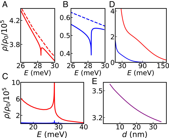
Fig. 4 shows the LDOS enhancement experienced by an emitter (or a nanosized tip) in the proximity of a superconductor; Fig. 4 A, B, D, and E refers to the case in the presence of graphene (located between the superconductor and the emitter), whereas Fig. 4C depicts a scenario where the graphene sheet is absent. The graphene sheet modifies the LDOS, affecting not only the absolute Purcell factor but also the peak/dip feature around the energy of the Higgs mode,


Purcell factor near a vacuum–hBN–graphene–hBN–superconductor heterostructure. In A and B the graphene Fermi energy has been set at
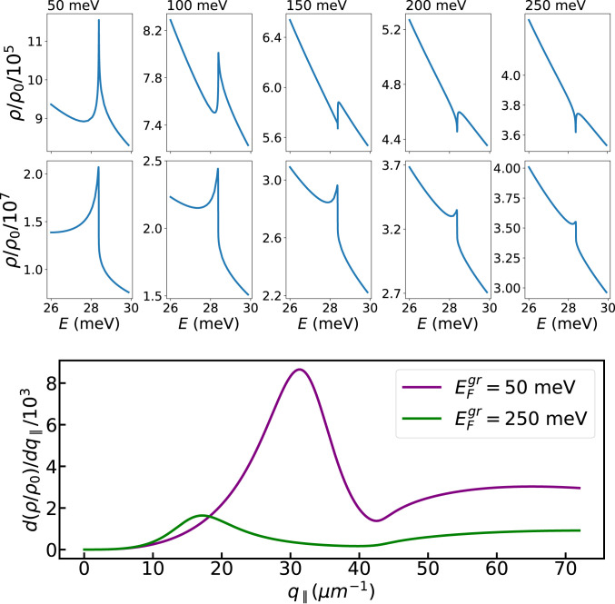
Finally, Fig. 5 depicts the LDOS enhancement for different values of graphene’s Fermi energy (which can be tuned electrostatically), for two fixed emitter–graphene distances:


Purcell factor as a function of graphene’s Fermi energy. Here we show the effect of changing graphene’s Fermi energy (indicated at the top of each column) while keeping all other parameters fixed:
Conclusion and Outlook
We have shown that signatures of a superconductor’s Higgs mode can be detected by exploiting ultraconfined graphene plasmons supported by a graphene sheet placed in a superconductor’s proximity. In particular, the presence of the Higgs mode for
Experimentally, the GP–Higgs interaction can be investigated using state-of-the-art cryogenic scanning near-field optical microscopy (SNOM) (43). Alternatively, more conventional spectroscopies relying on far-field optical techniques can also be explored by nanopatterning the graphene itself (e.g., into ribbon arrays) or its nearby materials (for example, the hBN or the superconductor). Examples of the latter—which have the benefit of preserving graphene from nanofabrication-induced defects—include the configurations studied in refs. 25 and 32, while the former approach can still be pursued using cutting-edge electron-beam lithography (61). Another possibility is the use of highly localized, local back-gate-free graphene doping modulation by placing a pristine graphene sheet on a substrate with patterned
Finally, there are a number of open questions that can spur from this work; e.g., if conductive thin films were added in direct electrical contact with the superconductor, then bound Andreev quasiparticle states inside the superconducting energy gap can form, being solutions to the Bogolubov–de Gennes equations (63). Another enticing outlook is the prospect of using highly confined GPs for investigating Josephson plasma waves in layered high-
The work presented here sheds light on the fundamentals of collective excitations in architectures containing two-dimensional materials and superconductors and constitutes a proof-of-principle proposal, paving the way for prospective experimental investigations into the electrodynamics of superconductors using ultraconfined graphene plasmons.
Acknowledgements
N.M.R.P. acknowledges support from the European Commission through the project “Graphene-Driven Revolutions in Information and Communication Technology (ICT) and Beyond” (881603–Core 3) and the Portuguese Foundation for Science and Technology (FCT) in the framework of the Strategic Financing UID/FIS/04650/2019. N.M.R.P. also acknowledges COMPETE2020, PORTUGAL2020, Fundo Europeu de Desenvolvimento Regional (FEDER), and the Portuguese FCT through Project POCI-01-0145-FEDER-028114. N.A.M. is a VILLUM Investigator supported by VILLUM FONDEN (Grant 16498) and Independent Research Fund Denmark (Grant 7026-00117B). The Center for Nano Optics is financially supported by the University of Southern Denmark (SDU) (SDU 2020 funding). The Center for Nanostructured Graphene is sponsored by the Danish National Research Foundation (Project DNRF103). Work on hybrid heterostructures at Columbia was supported entirely by the Center on Precision-Assembled Quantum Materials, funded through the US National Science Foundation Materials Research Science and Engineering Centers (Award DMR-2011738). D.N.B. is Moore Investigator in Quantum Materials, Emergent Phenomena in Quantum Systems (EPiQS) 9455. D.N.B. is the Vannevar Bush Faculty Fellow ONR-VB: N00014-19-1-2630. F.H.L.K. acknowledges financial support from the Government of Catalonia trough the SGR grant and from the Spanish Ministry of Economy and Competitiveness (MINECO) through the Severo Ochoa Program for Centers of Excellence in Research & Development (SEV-2015-0522); support by Fundació Cellex Barcelona, Generalitat de Catalunya through the Centres de Recerca de Catalunya (CERCA) program; and the MINECO grants Plan Nacional (FIS2016-81044-P) and the Agency for Management of University and Research Grants 2017 SGR 1656. Furthermore, the research leading to these results has received funding from the European Union’s Horizon 2020 program under the Graphene Flagship Grants 785219 (Core 2) and 881603 (Core 3) and the Quantum Flagship Grant 820378. This work was also supported by the European Research Council (ERC) TOPONANOP under Grant 726001.
Data Availability.
All study data are included in this article and/or SI Appendix.
References
1
2
3
4
5
6
7
8
9
10
11
12
13
14
15
16
17
18
19
20
21
22
23
24
25
26
27
28
29
30
31
32
33
34
35
36
37
38
39
40
41
42
44
45
46
48
49
50
51
52
53
54
55
56
57
58
59
60
61
62
63
64
65
 Harnessing ultraconfined graphene plasmons to probe the electrodynamics of superconductors
