Nano Letters

- Altmetric
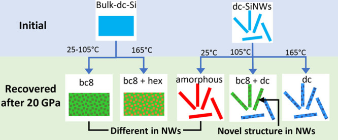
Silicon has several technologically promising allotropes that are formed via high-pressure synthesis. One of these phases (hd) has been predicted to have a direct band gap under tensile strain, whereas other (r8 and bc8) phases are predicted to have narrow band gaps and good absorption across the solar spectrum. Pure volumes of these phases cannot be made using conventional nanowire growth techniques. In this work, Si nanowires were compressed up to ∼20 GPa and then decompressed using a diamond anvil cell in the temperature range of 25–165 °C. It was found that at intermediate temperatures, near-phase-pure bc8-Si nanowires were produced, whereas amorphous Si (a-Si) dominated at lower temperatures, and a direct transformation to the diamond cubic phase (dc-Si) occurred at higher temperatures under compression. Thus this study has opened up a new pressure–temperature pathway for the synthesis of novel Si nanowires consisting of designed phase components with transformative properties.
Creating exotic phases of materials using pressure is a topic of strong scientific and technological interest. There are at least 14 different phase of silicon that can be formed via the application of high pressure, including several phases that have very compelling properties.1,2 For example, a body centred cubic phase (bc8-Si, Ia3̅) was recently reported to be a very narrow (0.03 eV) direct band gap semiconductor,3 bc8-Si nanoparticles have been predicted to be promising candidates for multiple exciton generation solar energy conversion,4 and r8-Si is predicted to have an indirect band gap of 0.24 eV and exhibit better absorption of the solar spectrum than dc-Si.5 Furthermore, the hd-Si phase is reported to be an indirect band gap (∼0.6 eV) semiconductor,6 but under more than ∼4% tensile strain, its band gap is predicted to become direct,7 and thus it is a promising candidate for a range of novel Si devices. All of these phases can be accessed via high-pressure synthesis; however, creating pure structures of these phases from bulk material is not possible and is difficult on the nanoscale due to amorphous Si (a-Si) being the dominant end phase.8,9
When bulk Si with its diamond cubic structure (dc-Si, Fd3̅m) under ambient conditions is loaded to ∼11 GPa, it transforms to a metallic phase with a β-Sn structure ((β-Sn)-Si, I41/amd).10,11 When pressure is further increased, (β-Sn)-Si will undergo reversible phase transformations to an orthorhombic structure (Imma-Si) at ∼13 GPa and then to a simple hexagonal structure (sh, P6/mmm) at ∼15 GPa,12 followed by other metallic phases.13,14 The dc-Si to (β-Sn)-Si phase transformation is not reversible at ambient temperature.15 In bulk Si, on decompression to ∼8 GPa, (β-Sn)-Si transforms to a rhombohedral structure (r8-Si, R3̅) and then to a bc8-Si at 3 GPa, which is the final phase at ambient pressure.15−17 When the bc8 phase is heated to ∼200 °C, it transforms into a hexagonal diamond (hd-Si, P63/mmc) structure,15,18 indicating the thermal stability of the metastable bc8-Si under modestly high temperature conditions.
Particle size is an important factor in synthesizing novel materials, including those with desired combinations of allotropes. Chemical syntheses of small bc8-nanoparticles have been reported with a diameter of <10 nm.19 If Si nanowires (NWs) composed of novel exotic allotropes could be prepared, then this would add considerably to their functionality. NWs are envisaged to have high potential for technological applications such as for biosensors and high-efficiency solar cells.20,21 However, it is not currently possible to produce the exotic r8 or bc8 phases in SiNWs by conventional NW growth methods, although hd-Si regions can be formed within dc-SiNWs by introducing compressive stresses within a surrounding matrix, by chemical vapor deposition, or by heteroepitaxial growth,22−24 noting that the latter method results in impurities that can compromise the desired properties. In fact, recent work on hd-Si NWs showed that mixing with Si’s sister element Ge can allow for the controlled formation of a direct band gap.25 However, none of these techniques yielding SiNWs of or with the hd phase can, to date, yield bc8-Si or r8-Si. Thus to produce pure phases of these exotic structures, a new approach is required. Clearly, one approach is to transform dc-SiNWs using pressure pathways to the desired end phase. So far, this approach has not succeeded at room temperature. In fact, in a recent study on the same of type SiNWs, it has been found that the dominant end phase is always amorphous (a-Si) at room temperature.8 This behavior is in contrast with that of bulk-Si, where bc8-Si is readily formed. The different NW behavior was explained in terms of nucleation retardation, where the small volume of the SiNWs suppressed the nucleation of r8-Si and subsequently bc8-Si during decompression.20 Such suppression of nucleation is presumably similar to that observed in bulk-Si during ultrarapid decompression26,27 or at low temperature,28,29 where a-Si is the resultant end phase. To promote the nucleation of exotic crystalline phases in such SiNWs, as studied previously, this current study adds an elevated temperature during the decompression of the SiNWs to overcome the kinetic barriers to aiding the nucleation of bc8/r8-Si.
Single-crystal SiNWs with a diameter of 80–150 nm were grown on a (110) Si substrate by the vapor–liquid–solid method using gold nanoparticle seeds for growth.30 The Au seeds were subsequently removed after growth in a two-stage process: removal of the oxide using hydrofluoric acid and then removal of the Au using an aqua regia solution. Transmission electron microscope (TEM) images of these SiNWs are shown in Supplementary Figure 1 of the Supporting Information. The SiNWs were then removed (well after the removal of the Au) from the substrate with a razor blade and placed into a diamond anvil cell (DAC) and gas-loaded at GSECARS with a Ne pressure medium.31 Pressure was remotely controlled using a double-membrane system.32 The pressure was increased to 20–22 GPa to fully induce the transformation to the metallic phases, in particular, to the sh structure.8 The metallic Si was then decompressed to ∼9 GPa (where the Si was still in the β-Sn phase) and then slowly decompressed at ∼2 GPa/h until ∼3 GPa. All of these compression and decompression experiments were performed at elevated temperatures, with the DACs heated using resistive heating to 70, 105, 135, and 165 °C. Another sample was compressed and decompressed at room temperature for comparison. Similar experiments were performed at 105 and 165 °C for bulk-Si (∼15 μm thick single crystal sample), also for comparison purposes. The samples were recovered from the DAC after decompression to ambient pressure for further analysis. X-ray diffraction (XRD) patterns were collected at HPCAT’s 16ID-B beamline at the Advanced Photon Source at Argonne National Laboratory for both the initial SiNW sample and the recovered DAC samples at energies of 31 (SiNWs) and 25 keV (bulk). The X-ray beam size was 3 × 6 μm2 full width at half-maximum (fwhm) in the vertical and horizontal directions, respectively, and thus the XRD covered a diffraction volume containing many individual NWs. In situ XRD measurements at 105 °C of SiNWs during both compression and decompression were also collected to monitor phase transitions (different sample than the ex situ measurements). For these in situ measurements, the pressure was determined by fitting the {111} peak of a Pt pressure marker that was placed into the cell and using the equation of state of Pt.33 Such in situ measurements ensured that the maximum pressure during compression was sufficient to transform all of the dc-SiNWs to metallic phases before decompression. Upon decompression, the in situ measurements also allowed any suppressed nucleation of all crystalline phases to be examined for the SiNWs and compared with bulk-Si. Decompression occurred at a rate of ∼30 GPa/h. Subsequently, the recovered SiNW samples were examined and confirmed to maintain the NW geometry with TEM in a Hitachi HF3300 operated at 300 kV. A more detailed description of the experimental procedure is given in the Supporting Information.
Figure 1a shows the end phases in bulk-Si after compression and decompression at the temperatures indicated. The final phase shown in Figure 1a is mostly bc8-Si up to 105 °C, but at higher temperatures, hd-Si is also observed (along with traces of dc-Si at 165 °C). Figure 1b shows representative integrated XRD patterns of the SiNWs before and after compression. For the compressed SiNWs, the temperature during compression and decompression is indicated. Multiple SiNWs are sampled simultaneously by the X-ray beam, and hence these results do not imply that the recovered SiNWs are mixed-phase. Before any pressure is applied, the SiNWs have sharp reflections corresponding to dc-Si. The diffraction pattern of SiNWs compressed at room temperature has broad features after decompression centered at Q = ∼2.01 and 3.47 Å–1 as well as several low-intensity sharper peaks. The broad features indicate the presence of amorphous Si (a-Si), and the weak sharper peaks can mainly be indexed to bc8-Si but with some peaks from dc-Si. Diffraction from a-Si should be much weaker than that from any of the crystalline phases, therefore the intense broad features suggest that these SiNWs are predominately a-Si, with a small fraction of bc8-Si and trace amounts of dc-Si. Neither dc-Si nor a-Si is formed in bulk-Si at this temperature under similar decompression conditions.

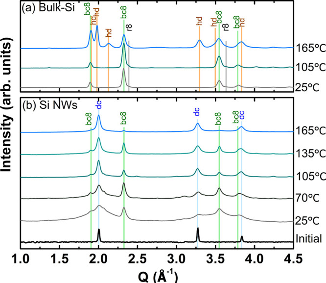
Integrated 1D X-ray powder diffraction patterns taken at ambient pressure and temperature of various samples recovered from DACs. Each sample was subjected to compression to ∼20–22 GPa and decompression at a rate of 2 GPa/h between 9 and 3 GPa at the indicated temperature and then recovered from the DAC after decompression. (a) Bulk-Si and (b) 80–150 nm SiNWs.
Increasing the temperature to 70 °C resulted in less a-Si and a higher fraction of bc8-Si and dc-Si. When the temperature was further increased to 105 °C (and 135 °C), all recovered SiNWs appear predominately crystalline, with the fraction of each of the bc8 and dc end phases being roughly similar (based on the peak intensities of these phases). The amounts of each of these phases varied across the recovered sample. It is interesting to note that dc-Si forms at these elevated temperatures in the NWs but not until ∼170 °C in bulk-Si29 or at ∼260 °C when formed from r8-Si under high pressure.34
The in situ XRD data from the SiNWs under pressure at 105 °C are shown in Figure 2. Here the dc-SiNWs transformed completely to sh-Si on compression (Figure 2a). On decompression (Figure 2b), the sh-Si transformed to (β-Sn)-Si; then, the β-Sn-Si transformed to both dc-Si and bc8/r8-Si between 9.3 and 7.9 GPa, with a small amount of dc-Si forming before any bc8/r8-Si. Because of the low intensity of the bc8/r8 peaks, it is not possible to unambiguously identify one phase over the other. However, on the basis of the transformation behavior of bulk-Si in the literature,17 r8-Si is more likely to be present. This r8-Si is then expected to transform to bc8-Si at lower pressures, and hence bc8-Si remains as the final phase after complete decompression. To identify the specific phases shown in Figure 2, the peaks were matched to the known positions from the literature.16,17,35

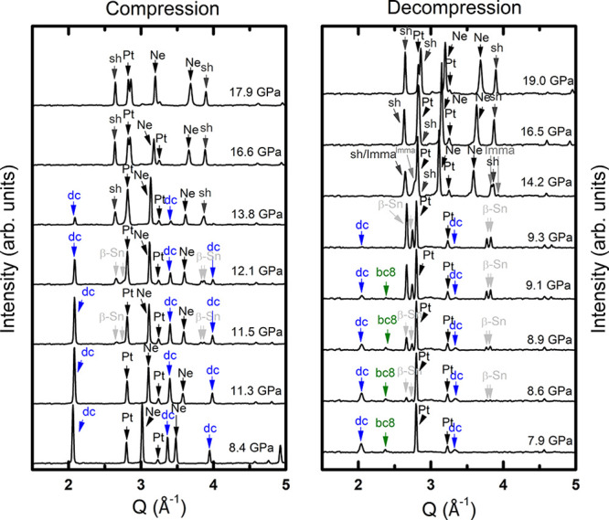
In situ XRD data of SiNWs under pressure at 105 °C during (a) compression and (b) decompression.
When the temperature was further increased to 165 °C, the formation of dc-Si dominated, and only a small fraction of bc8-Si was formed in the NWs (Figure 1b). It is possible that some hd-Si was formed, but because of the overlap of the main hd-Si peaks with some of those of bc8-Si and dc-Si, no clear evidence of the hd phase can be concluded. The behavior differs from that of bulk-Si, where hd-Si was observed in this study and also in the past studies when annealing bc8/r8-Si under pressure.34
It is clear that the final phases present after the decompression of SiNWs significantly differ from those of bulk-Si. These differences are presumably a result of the suppressed nucleation of the exotic crystalline phases in the SiNWs, presumably due to the small volume and hence the high surface-to-volume ratio.8 To further understand the XRD results, which measure many SiNWs simultaneously, the microstructure and phases present in individual SiNWs were studied by TEM (at CNMS, ONRL). This allows for the imaging and diffraction of individual SiNWs and thus allows for the investigation of phase purity. In general, the TEM images of individual NWs showed that they mainly appear in single phases—a-Si, bc8-Si, or dc-Si. Crystalline SiNWs were found to be polycrystalline. However, for the specimens held at intermediate temperatures (70–135 °C), in particular, there was typically a distribution of these phases in the SiNWs at each temperature, which is consistent with the XRD data.
Figure 3 shows a collage of TEM micrographs and selected area diffraction patterns of the recovered samples. Additional TEM images are located in the Supporting Information. Figure 3a shows a dark-field (DF) image, taken with the objective aperture positioned over the encircled spot in the inset selected area electron diffraction (SAED) pattern, of a group of SiNWs that were compressed at room temperature. The SAED of these SiNWs contains amorphous rings and several weak spots. These spots were mostly indexed to dc-Si (labeled on the figure with semicircles); however, some bc8-Si was also observed. The encircled spot is one of the {111} dc-Si reflections, and its DF image shows that dc-Si is predominately found in one of the SiNWs. The other SiNWs in this image are mostly or entirely amorphous. (The amount of a-Si in each SiNW varied significantly from entirely a-Si to mostly crystalline.) Another group of SiNWs compressed under these conditions (not shown) was observed to contain both bc8-Si and a-Si. It thus appears that compressing SiNWs at room temperature gives NWs that are either entirely amorphous, a mixture of a-Si and some bc8-Si, or a mixture of a-Si and some dc-Si. These TEM data provide the microstructures of the SiNWs, whereas the XRD data provide an averaged phase distribution over all SiNWs with the dominant a-Si phase and trace amounts of bc8-Si and dc-Si.

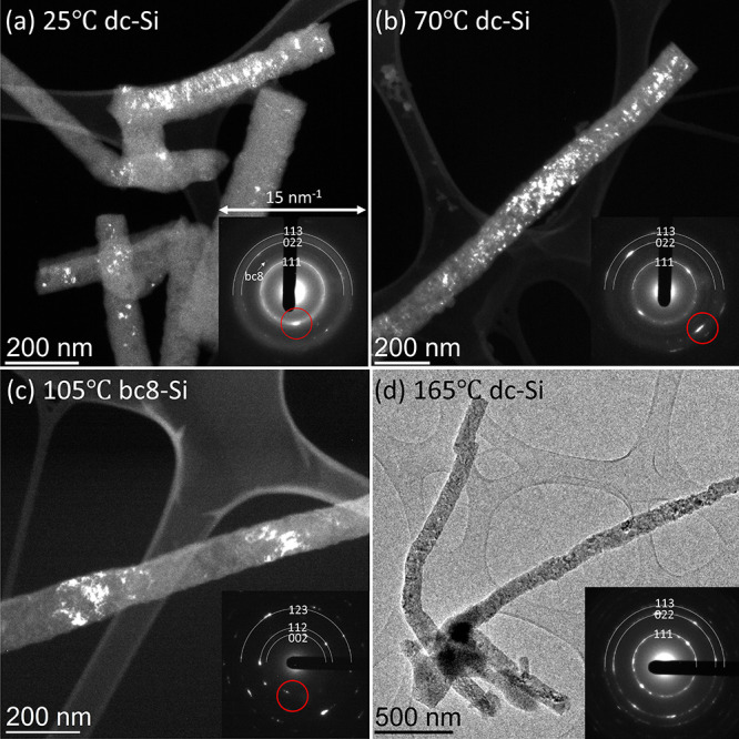
TEM micrographs and inset SAEDs of SiNWs decompressed at different temperatures. Dark-field images of nanowires compressed at (a) 25 °C that contain dc-Si, (b) 70 °C that contain dc-Si, and (c) 105 °C that contain bc8-Si. (d) Bright-field image of nanowires compressed at 165 °C containing dc-Si. Note that all SAEDs have a width of 1.5 Å–1.
The SiNWs that were compressed at 70 °C were found to be mostly polycrystalline bc8-Si or dc-Si (both with traces of a-Si). An example of a SiNW that was compressed at 70 °C is shown in Figure 3b, where the SiNW is observed to be polycrystalline dc-Si. It appears that unlike at room temperature, no completely amorphous SiNWs formed, which is again consistent with the XRD data. In addition, the SiNWs that were compressed at 105 °C contained individual SiNWs that were predominately bc8-Si but also some that were dc-Si. Figure 3c shows a DF image of a SiNW that was compressed at 105 °C and was found to be bc8-Si. The inset SAED contains no clear a-Si rings. Indeed, the dc-SiNWs formed from (β-Sn)-Si at this temperature were also found to be polycrystalline. Consistent with the XRD data, no entirely amorphous SiNWs were detected. Figure 3d shows an example of a SiNW that was compressed at 165 °C. This SiNW contained polycrystalline dc-Si, consistent with XRD data where dc-Si was the dominant phase. The final phase of individual SiNWs did not appear to be dependent on the thickness of the SiNWs in the 90–150 nm diameter size range as both bc8-Si and dc-Si were observed for multiple diameters. The mechanisms behind this behavior are unclear, but it should be noted that the transformation from (β-Sn)-Si to dc-Si is not observed in bulk material.
The key observations from this temperature-dependent phase transformation study of SiNWs and bulk-Si are summarized in Table 1. From this table, it is quite clear that the phases formed in bulk-Si and SiNWs differ markedly, where at room temperature, a-Si is dominant for SiNWs compared with bc8-Si for bulk-Si. Furthermore, dc-Si forms in addition to bc8-Si at higher temperatures for the SiNWs but not for bulk-Si. As previously indicated, this difference is likely to be a result of the suppressed nucleation of exotic crystalline phases in the case of SiNWs, presumably due to their small volume and hence large surface-to-volume ratio. Such nucleation difficulties also arise on compression: Suppression of (β-Sn)-Si formation occurs; instead, there appears to be a direct transformation from dc-Si to sh-Si between 15 and 22 GPa.8 Difficulty in nucleating r8/bc8 phases on decompression results in (β-Sn)-Si persisting until ∼5 to 6 GPa.8,36 This behavior accounts for the complicated transformation pathways for SiNWs on decompression, where unstable (β-Sn)-Si can transform to one of three phases depending on the pressure and the available nucleation sites: a-Si, bc8-Si, or dc-Si. The detailed mechanisms behind this effect are not clearly illustrated by this current data set and are a topic of future work.

| temperature | bulk | 80–150 nm Si nanowires |
|---|---|---|
| ambient | bc8-Si (trace r8) (polycrystalline) | a-Si |
| 70 °C | not measured but presumed bc8-Si as at higher and lower T | bc8-Si (some dc-Si) (polycrystalline) (trace a-Si) |
| 105 °C | bc8-Si (trace r8) (polycrystalline) (β-Sn)-Si to r8-Si at ∼10.4–8.4 GPa34 r8 to bc8 at 3–2 GPa (ambient temperature)16 | bc8-Si + dc-Si (polycrystalline) (β-Sn)-Si to bc8 or r8-Si at 9.3–7.9 GPa |
| 165 °C | bc8-Si + hd-Si (polycrystalline) | predominately dc-Si (polycrystalline) |
On the basis of the results of this study and literature reports, Figure 4 shows a schematic that summarizes the phase transformation pathways in bulk-Si and SiNWs. The bulk-Si results are consistent with previous studies. For SiNWs, the nucleation of new crystalline phases from (β-Sn)-Si during decompression is substantially suppressed, and this behavior is clearer at lower temperatures. Because of the nucleation difficulties, (β-Sn)-Si becomes more unstable as pressure is reduced, and hence the driving force for phase transformation increases. At ambient temperature, some (β-Sn)-Si phase remains down to ∼5 to 6 GPa, which is 3 to 4 GPa below the lower bound of its stability range in bulk-crystal-Si.1 At this pressure, because no crystalline structure has yet formed, a-Si is favored. Note that even when crystalline metastable phases nucleate (in a few SiNWs), a-Si is also found to form in the same SiNW, possibly suggesting that growth is suppressed. During decompression at intermediate temperatures, transformation to bc8/r8 is no longer fully suppressed, as more thermal energy is available to assist the nucleation and growth of crystalline phases (r8-Si and dc-Si).

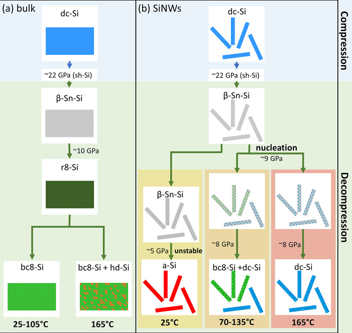
Schematic of the pressure-induced transformations in (a) bulk-Si and (b) SiNWs and their temperature dependence.
Now we turn to examine the various transformation pathways for NWs on decompression at elevated temperature in terms of thermodynamic and kinetic considerations. Rapp et al.37 and Mujica et al.38 have plotted the relative enthalpy of various allotropes of Si with respect to bc8-Si as a function of pressure. These studies show that if there were no kinetic barriers to phase transformation, then the (β-Sn)-Si phase would, on decompression, directly transform to dc-Si at a pressure of ∼10 GPa. This has indeed been reported for bulk Si above 170 °C.29,34 However, normally, the kinetic barrier to the nucleation of dc-Si is high,39 and this phase does not form at lower temperatures. Instead, structures with higher enthalpy but lower kinetic barriers form under particular conditions, for example, r8, bc8, and a-Si. Indeed, other than dc-Si and hd-Si, r8-Si has the lowest enthalpy between about 10 and 2 GPa,37 which is consistent with (β-Sn)-Si transforming to this phase at ∼9 GPa in bulk Si, then transforming to bc8-Si at ∼2 GPa, where this phase has a lower enthalpy. Wang et al.39 previously argued that the barrier to bc8 formation is much smaller than that of dc-Si and that this is the reason bc8-Si, not dc-Si, is the dominant end phase after decompression when bulk Si is the starting material. It is somewhat surprising that SiNWs directly transform from (β-Sn)-Si to dc-Si. However, the suppression of phase formation under decompression of NWs yields supercritical (β-Sn)-Si as pressure is reduced, and if sufficient thermal energy is available (at elevated temperatures), then the barriers to formation of all crystalline phases may be significantly reduced, allowing them to nucleate. In this scenario, the direct formation of the lowest enthalpy dc-Si phase might be anticipated at higher temperatures. Note that in our case, dc-Si is the dominant end phase at 165 °C. In addition, if small dc-Si crystallites do nucleate on decompression, then they might be expected to grow under the effect of both pressure and elevated temperature, noting that it has previously been shown that quite modest pressures of 2 GPa can enhance the growth rate of crystalline Si from a-Si by more than an order of magnitude.40,41 We suggest that this scenario is the explanation for a predominantly dc-Si end phase at 165 °C and for significant amounts of dc-Si at lower temperatures. Furthermore, as the temperature is reduced and the barrier to dc-Si formation becomes more significant, it may be more energetically favorable for r8 and bc8-Si to nucleate from unstable (β-Sn)-Si, as we observe. Finally, if the nucleation of all crystalline end phases is suppressed, particularly at the lowest temperatures, then this may lead to transformation to an amorphous phase, which is consistent with our observation of an increasing fraction of a-Si as the temperature is reduced and for a dominant a-Si end phase at ambient temperature.
The formation of a-Si under pressure warrants some comment because at equilibrium, most forms of a-Si have a lower density than dc-Si,42 and it might be expected to be difficult to form from a dense metallic (β-Sn)-Si phase under pressure. However, it has been shown in early DAC studies that a-Si can have a high-density form under pressure43−45 and when recovered from high pressure.46 Furthermore, the rapid decompression of a DAC has also been observed to result in a-Si in the case of a bulk Si starting material,26,27 and it may well be that this phase is considerably more dense than a-Si formed at ambient pressure. In addition, it is interesting that using another method of inducing phase transformations in small material volumes, namely, nanoindentation, can induce a-Si to form from (β-Sn)-Si during moderate unloading rates.47−49 It may be interesting to compare the transformation behavior of SiNWs under pressure with nanoindentation-induced transformations at similar material volumes and as a function of temperature due to the differing stress states.
This study opens the prospect of using bc8-SiNWs (and possibly hd-SiNWs) for technological applications, as their properties in near-phase-pure NWs can now be measured. For example, bc8-Si nanoparticles are predicted to be useful for multiple exciton generation solar energy conversion,4 and hd-Si is predicted to have a direct band gap when strained.7 For the latter to be realized, it would be important to study the behavior of bc8-SiNWs at elevated temperatures to determine if they transform to the hd-Si phase, as observed in bulk-Si.18
In conclusion, it is clear that in the 25–165 °C temperature range studied, SiNWs exhibit different phase transformation behavior to bulk-Si on decompression due to a retarded nucleation of exotic crystalline end phases. However, bc8-Si can be formed in individual SiNWs, in particular, in the 70–135 °C temperature range. At lower temperatures, a-Si is the dominant end phase, whereas dc-Si dominates at 165 °C. These results pave the way for producing and measuring the properties of near-phase-pure bc8-SiNWs.
Supporting Information Available
The Supporting Information is available free of charge at https://pubs.acs.org/doi/10.1021/acs.nanolett.0c04354.
Detailed description of the experimental method and some additional TEM images of the SiNWs and electron diffraction patterns (PDF)
Author Present Address
# L.Q.H.: Shock and Detonations Physics (M-9), Los Alamos National Laboratory, Los Alamos, New Mexico 87545, United States.
Author Contributions
L.Q.H., A.L., J.E.B., and J.S.W. conceived the idea for this research. A.L. grew the nanowires. L.Q.H. performed the diamond anvil cell experiments and XRD measurements under the supervision of G.S. and in discussion with B.H. D.A.C. performed the transmission electron microscopy with L.Q.H. All authors contributed to the discussion and preparation of the manuscript.
Notes
The authors declare no competing financial interest.
Acknowledgments
We thank Brett Johnson from the University of Melbourne for removing the Au from the nanowires. We also thank Rostislav Hrubiak, Jesse Smith, and Curtis Kenney-Benson from HPCAT for their technical assistance. We also thank Sergey Takchev for the gas loading. L.Q.H. was supported by an Australian Government Research Training Program Scholarship, and some travel support was provided by the Australian Nanotechnology Network through an Overseas Travel Fellowship. B.H. was supported by resources at the Spallation Neutron Source (SNS) and the High Flux Isotope Reactor (HFIR), DOE Office of Science User Facilities operated by the Oak Ridge National Laboratory (ORNL). We acknowledge the use of HPCAT facilities. HPCAT operations are supported by DOE-NNSA’s Office of Experimental Sciences. Use of the COMPRES-GSECARS gas loading system was supported by COMPRES under NSF Cooperative Agreement EAR-1606856 and by GSECARS through NSF grant EAR-1634415 and DOE grant DE-FG02-94ER14466. This research used resources of the Advanced Photon Source, a U.S. Department of Energy (DOE) Office of Science User Facility operated for the DOE Office of Science by Argonne National Laboratory under contract no. DE-AC02-06CH11357. Electron microscopy was conducted at the Center for Nanophase Materials Sciences (CNMS2017-038), which is a DOE Office of Science User Facility. We acknowledge the facilities and the scientific and technical assistance of Microscopy Australia at the Centre for Advanced Microscopy, Australian National University, a facility that is funded by the University and the Federal Government. We gratefully acknowledge financial support by the Austrian Science Fund (FWF), project no. P28175-N27 and the Australian Research Council Discovery Project Scheme (DP140102331).
 Synthesis of Novel Phases in Si Nanowires Using Diamond
Anvil Cells at High Pressures and Temperatures