 Light Emission in Metal–Semiconductor Tunnel
Junctions: Direct Evidence for Electron Heating by Plasmon Decay
Light Emission in Metal–Semiconductor Tunnel
Junctions: Direct Evidence for Electron Heating by Plasmon Decay
Nano Letters


- Altmetric
We study metal–insulator–semiconductor tunnel junctions where the metal electrode is a patterned gold layer, the insulator is a thin layer of Al2O3, and the semiconductor is p-type silicon. We observe light emission due to plasmon-assisted inelastic tunneling from the metal to the silicon valence band. The emission cutoff shifts to higher energies with increasing voltage, a clear signature of electrically driven plasmons. The cutoff energy exceeds the applied voltage, and a large fraction of the emission is above the threshold, ℏω > eV. We find that the emission spectrum manifests the Fermi–Dirac distribution of the electrons in the gold electrode. This distribution can be used to determine the effective electron temperature, Te, which is shown to have a linear dependence on the applied voltage. The strong correlation of Te with the plasmon energy serves as evidence that the mechanism for heating the electrons is plasmon decay at the source metal electrode.
Electrically driven plasmonic devices have gained recent interest due to the unique opportunity they offer to tune the emitted spectrum through applied voltage.1−4 This may be applied to on-chip communication5,6 and also serve as a research tool, allowing access to dark plasmonic modes that are not accessible through external optical excitation.7 The general idea that light can be generated in metal–insulator–metal tunnel junctions was first demonstrated more than four decades ago.8−10 A renewed interest in this phenomenon was sparked in the early 1990s, when light emission was reported in scanning tunneling microscopy (STM) experiments.11,12 Recent technological advances in nanometer-scale fabrication and the discovery of new materials (i.e., 2D materials) introduced rich platforms for further study and utilization of this phenomenon.13
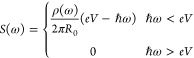
Early studies led to a relatively simple and straightforward model for light emission in tunnel junctions:16,17 electrons that tunnel from occupied states in one electrode to unoccupied states in the second electrode may lose their excess energy through excitation of a plasmon (either localized or propagating surface plasmon (SP)), which may consequently be scattered into free-space detectable photons. The spectrum of this plasmonic excitation can be derived from the noise power spectrum, Iω, of the tunneling current, where the Poissonian statistics of the tunneling events is manifested as time-dependent fluctuations, or equivalently, using Fermi’s golden rule. Accordingly, one may express the noise power as

This simplified derivation was challenged by numerous reports of above-threshold light emission (ATLE), where ℏωmax > eV. STM experiments showed evidence for ℏωmax = 2eV,12,19,20 and a model suggesting correlated tunneling of two electrons, which interact with a plasmon-polariton mode, was shown to reproduce the experimental data. Measurements of the ATLE intensity, performed on metallic break-junctions, found that it scales with √P, where P = IV is the electrical power.21 This observation led the researchers to conclude that the ATLE is due to blackbody radiation of the electron gas of the drain electrode. It was argued that the elevated temperatures are caused by the dissipation of the energy carried by the tunneling electrons.
On the other hand, a recent study done on ensembles of break-junctions of different metals showed that the electron-gas effective temperature, Te, depends linearly on the applied voltage.22 This linear dependence led the authors to suggest that the heating of the electrons is due to a nonradiative decay of electrically excited localized plasmons at the drain electrode. It was argued that this decay excites an electron above the metal Fermi energy, EF, thus creating electron and hole gases, each having a Boltzmann distribution with higher effective temperature. Accordingly, the light emission mechanism is not blackbody radiation, but rather the recombination of these hot electrons and holes.
In this work, we revisit this problem by studying light emission in a metal–insulator–semiconductor (MIS) tunnel junction under a reversed bias condition; more explicitly, electrons are injected from the metal to the semiconductor. In contrast to previous ATLE measurements, conducted in STM or break junction systems, the MIS structure allows us to define a clear plasmon resonance and study separate processes that occur in the source and in the drain. We show that this structure gives rise to light emission by inelastic tunneling of metal electrons to the semiconductor valence band, a significant part of which appears at above-threshold energies, ℏω > eV. The existence of ATLE in this structure, where there are no electrons to heat in the drain, allows us to refute the models attributing the heating to interactions of the tunneling electrons21 or plasmons22 with the electron gas in the drain. Instead, we show that the ATLE manifests the high-energy tail of the Fermi–Dirac distribution of the electrons at the metal electrode, which, in our case, is the source electrode. We find that the temperature of these electrons, Te, scales linearly with voltage as long as the emission cutoff energy is within the broad plasmon bandwidth. At higher voltages, Te exhibits a much smaller dependence on voltage and increases at a slower rate. We show that this finding implies that electron heating is caused by plasmons that give their energy to the metal electron bath.
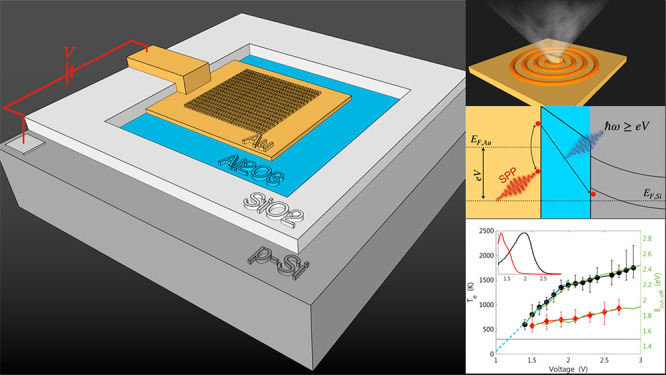
The structure we use is depicted in Figure 1a. It consists of a p-type silicon substrate (Na = 1 × 1015 cm–3), a 3 nm Al2O3 barrier deposited by atomic layer deposition (ALD), and a thermally evaporated 10 nm top gold electrode. We characterized the thickness of the oxide layer using ellipsometry (Woolam M-2000) and atomic force microscopy (Bruker Dimension Icon) and found good uniformity across the wafer (see Supporting Information). To ensure proper adhesion of the gold layer to the oxide barrier, a thin titanium layer of ∼1 nm is deposited before the gold evaporation. Since such an adhesion layer damps the plasmonic field,23,24 we attempted to make it as thin as possible. We note that, in our case, this damping could be even more critical since electron tunneling, which is the source of plasmon excitation in the gold layer, occurs from the titanium layer. Finally, a second patterned gold layer, made of nine periodic arrays, each 3 × 3 μm2, consisting of elongated bars with different bar periodicities, is deposited on the structure using electron-beam lithography. The width and thickness of the bars are 100 and 30 nm, respectively, and their lengths vary from 100 to 500 nm between different samples. The bars on the sample shown in this paper are of size 100 nm by 500 nm (Figure 1b), and measurements of other samples are shown in the Supporting Information. The structure is patterned to form a 10 × 10 μm2 mesa, with electrical contacts to the substrate and metal electrodes.

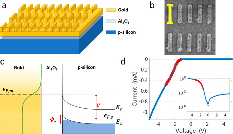
(a) A scheme of the sample structure. A p-type silicon substrate is coated with a 3 nm layer of Al2O3 using ALD and a 10 nm layer of gold using thermal evaporation. A periodic array of identical gold bars is fabricated using electron-beam lithography. The width and thickness of the bars are 100 and 30 nm, respectively, and their length varies from 100 to 500 nm in different devices. (b) A top-view SEM image of the bar pattern. The scale bar length is 500 nm. (c) A diagram of the band structure near the tunnel junction. ϵF,m and ϵF,s are the gold and silicon Fermi energies, respectively. V is the applied voltage, and ϕs is the surface potential in the silicon due to the band bending. In green is the Fermi–Dirac distribution function for a given effective temperature, Te. (d) A plot of the current vs voltage of the device. The inset shows the same data on a logarithmic scale. The red circles mark the voltage range at which light emission measurements were performed.
Figure 1c shows the band structure of the device under a reverse-bias condition. At large voltages, the silicon bands bend, and a hole-accumulation layer is formed near the barrier.25 At an applied voltage of 2–3 V, the band-bending region extends over ∼100 nm. Hence, the probability of ballistic transport of electrons, which tunnel through the conduction band barrier and releases their energy via photon emission, is very low. We also note that the indirect nature of the silicon band structure strongly inhibits light emission by electron–hole recombination in the semiconductor drain electrode. Hence, light emission in this structure can only occur through inelastic tunneling of electrons from the metal into the hole’s accumulation layer. At the opposite polarity, the current comes from the minority charge electrons at the semiconductor that flow to the metal electrode. In this case, the number of electrons that can tunnel is much smaller, and hence, no significant light emission is expected. Indeed, this asymmetry is well manifested in the current versus voltage curve (Figure 1d).
Let us now turn to the experimental results. Upon application of a negative voltage to the source, we observe the appearance of a large number of diffraction-limited bright spots on the mesa (Figure 2a). Their intensity increases linearly with the current through the device (see Supporting Information). We verified that when the polarity of the devices is reversed no light emission is observed at any voltage. We find a clear correlation between the appearance of spots and titanium layer thickness: The density of the emission spots and the yield of light-emitting devices increase as this layer is made thinner. At a layer thickness of ∼1 nm, about half of the measured devices show spotty light emission. We conclude that the presence of the adhesion layer suppresses light emission and suspect that the spots come from small regions where the gold layer is in direct contact with the oxide tunnel barrier.
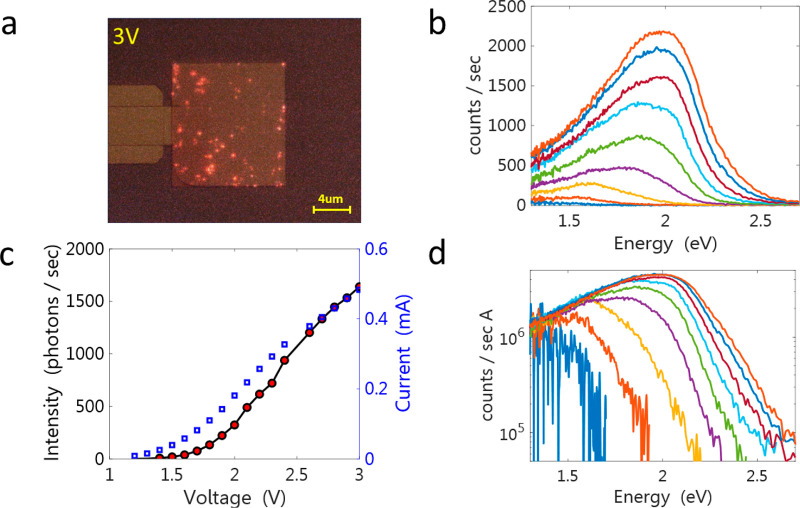
(a) An optical microscope image of the emission, which is taken in a dark ambiance and is superimposed on an image of the illuminated sample. The bright emitting spots are clearly visible. (b) The measured spectra (normalized by the camera response) under different applied voltages between 1.4 V and 3 V, in steps of 0.2 V. (c) The integrated light intensity (black-red) and the measured current (blue) as functions of the voltage. (d) The same spectra as in panel b plotted on a logarithmic scale and divided by the tunneling currents at the corresponding voltage. The blueshift of the cutoff energy with increasing voltage is clearly seen.
Figure 2b shows the measured spectra at various applied voltages for one of the measured devices. The variability of the spectra between the spots is rather small, and we present here the integrated signal from all of the spots. It is seen that, as the current through the device increases, the spectrum increases in amplitude (Figure 2c). A remarkable feature in the spectra, which is a well-known footprint of the electrically driven plasmon, is the shift of the cutoff energy to higher energies with voltage. In Figure 2d, we replot the spectra on a logarithmic scale and normalize each by the current at the corresponding voltage. It is seen that the spectra evolve under the envelope of the plasmon resonance (defined by the spectrum at high voltage), such that their low energy sides overlap and their cutoff energies, ℏωmax, shift to higher values with voltage. Examining devices with different patterns, we find that the emission line shape depends on the aspect ratio of the bars but not on the array periodicity, indicating that the electrically driven plasmon is localized.
In Figure 3, we show a few examples of the measured spectra, at V = 1.6, 1.8, 2.0, and 2.2 V, where the regimes in which ℏω > eV are shaded in red. A significant fraction of the emission spectrum resides at energies above the applied voltage. To analyze the spectral dependence on voltage, we factor out the contributions of the voltage-independent terms in the expression for the power spectrum. This is achieved by dividing each spectrum by the one measured at the highest voltage, V0 = 3 V, similarly to the normalization performed in refs (21) and (22). Indeed. It is evident from Figure 2b,d that, at high voltages, the emission spectrum ceases to change, and the plasmonic spectrum is fully recovered
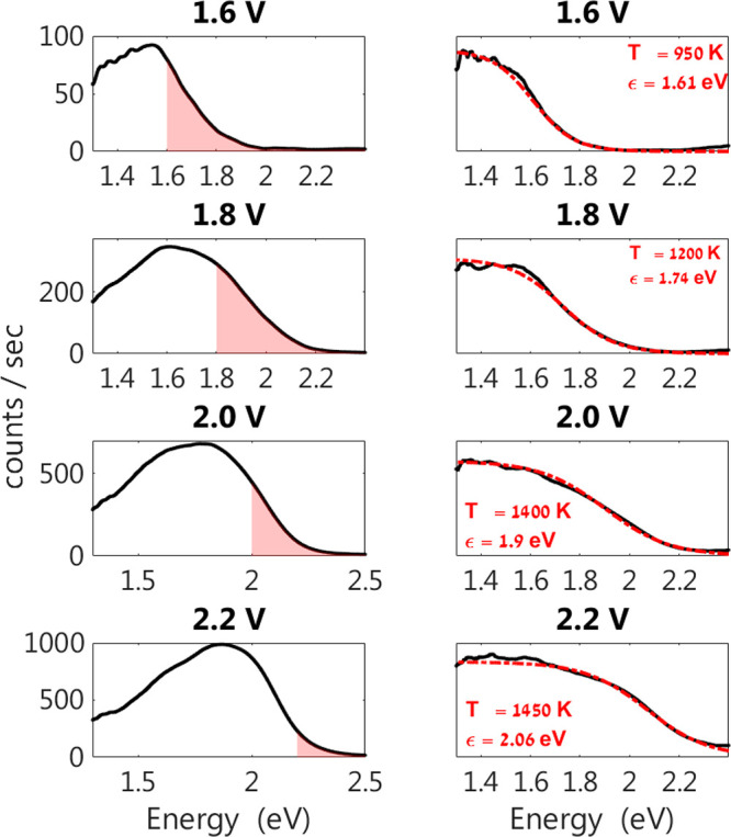
(Left panels) Measured spectra (normalized by the camera response) at several voltages between 1.6 and 2.2 V. The shaded areas mark the above-threshold light emission (ATLE). (Right panels) The spectra divided by the emission spectrum at 3 V (black) and the fits to a Fermi–Dirac distribution (dashed red). The fitted value of ε and Te are specified for each voltage.
It is easy to see that if we consider tunneling to the top of the silicon valence band only, this division should simply yield the Fermi–Dirac distribution of the electrons in the metal, .Here ε(V) = V + Δ – φs is the difference between the gold Fermi energy and the top of the silicon valence band (see Figure 1c), φs is the surface potential, Δ is the height of the silicon Fermi level above the valence band, and Te(V) is the electron temperature at that voltage. Since the surface hole density is relatively low, the distribution at the semiconductor side of the junction, 1 – f(Ej), could be well approximated by a step function. The right panels of Figure 3 show the corresponding divided spectra, together with the fits to f(ω,V). It is seen that a very good fit is obtained for all spectra.
The fits to a Fermi–Dirac function allow us to extract the values of ε and Te for each voltage. We find that ε(V) increases monotonously with voltage and gives rise to the blueshift of the emission spectrum with increasing voltage. We note, however, that there is a difference between ε(V) and the applied voltage, ε(V)-V = Δ – φs, due to the silicon band bending. Hence, this measurement allows us to determine the voltage dependence of the surface potential directly (see Supporting Information).
Let us turn now to examine the behavior of the electron temperature (Figure 4b). The black symbols are the calculated Te for the device described above. Two voltage regimes can be clearly identified: a low-voltage range, 1.4 < V < 2.0 V, where Te increases at a high slope, and a high-voltage range, 2.0 < V < 3.0 V, where the temperature increase with voltage is much slower. To understand this behavior, we compare it to the voltage dependence of ℏωmax, extracted from the spectra of the device depicted in Figure 2 and marked by the green line in Figure 4b. We note that while the determination of the cutoff energy is somewhat arbitrary, the result of this analysis is insensitive to the exact level at which we set the cutoff. It is clearly seen that as the applied voltage exceeds the peak of the plasmon spectrum at ∼2 eV, the blueshift of ℏωmax slows down considerably, limited by the sharp falling edge of the plasmon spectrum. This is in excellent correlation with the behavior of Te(V), therefore providing a clear indication for the mechanism responsible for ATLE: plasmon–electron interactions at the metal source electrode excite electrons above the Fermi level.26 These hot electrons quickly thermalize among themselves and form a Fermi–Dirac distribution at a temperature Te, which is higher than the lattice temperature.22 Since the quantum of energy that is given to the electron bath in such an interaction is proportional to the plasmon energy, we should get that kBTe ∝ ℏωmax, where kB is the Boltzmann constant. A confirmation for this interpretation is provided by the behavior of another device, in which the plasmon resonance is at much lower energy, 1.3 eV (red curve in the inset of Figure 4b). The electron temperatures for this device (red symbols) are much lower and its voltage dependence at V > 1.3 V is the same as the first device at voltages larger than the resonance, V > 2 V. This reaffirms the critical role of the plasmons in the electron heating (see further measurements in the Supporting Information).
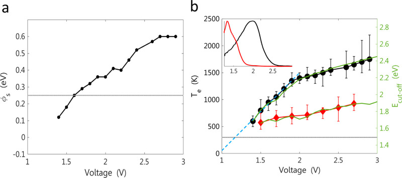
(a) Dependence of the surface potential, φs, on voltage. The gray line marks the Fermi energy with respect to the top of the bulk silicon valence band. (b) In black are the electron temperatures as derived from the fits to a Fermi–Dirac distribution for the device described in previous figures. In dashed blue is the linear extrapolation of the low-energy part of the curve. The crossing of the 300 K level (dashed gray line) is at 1.1–1.2 V. For comparison, in red are the effective electron temperatures of another device, with a distinct plasmon resonance at 1.3 eV. The green solid lines mark the dependence of ℏωmax on voltage. (It is set at the photon energy where the emission intensity drops to 10% of its maximal value.) The inset shows the normalized emission spectrum of the two devices (in arbitrary units) at high voltage.
A remarkable feature in Figure 4b is that, as the Te(V) curve is extrapolated to low voltages (dashed blue line), it crosses Te = 300 K at V ≈ 1.1–1.2 V, where the gold Fermi level is aligned with the silicon conduction band (Figure 1c). Under this condition, the electron wave function extends into the silicon conduction band, and its overlap integral with the hole wave function increases, giving rise to a sharp increase of the tunneling probability. It is easy to realize that the other inelastic tunneling process, by a deep electron from the gold layer to the silicon valence band, has a much lower probability. We can thus conclude that the onset of plasmon emission occurs at V ≈ Eg, where Eg is the silicon gap. The fact that this onset is manifested in the Te(V) curve provides strong confirmation of the validity of our analysis. We believe that this finding, together with the two-slopes behavior of Te(V) and the excellent fits to a Fermi–Dirac distribution, provides convincing evidence that the mechanism for ATLE is heating of the electron bath by plasmon decay.
In the concluding part of this paper, we wish to comment on the potential applications of our findings. The realization of a silicon-based light-emitting device, where the applied voltage determines the emission spectrum, may allow easy integration of photonic devices in integrated circuits. Such tunnel devices can be switched at very high speed and miniaturized to a size of a few nm, compatible with the demands of silicon electronics.
Supporting Information Available
The Supporting Information is available free of charge at https://pubs.acs.org/doi/10.1021/acs.nanolett.0c03945.
Descriptions of device fabrication process, barrier deposition and characterization, bands structure calculation, spectroscopy of individual spots, data from other devices, and spectrum reconstruction (PDF)
Notes
The authors declare no competing financial interest.