Nature Communications
Home Efficient phonon cascades in WSe2 monolayers
Efficient phonon cascades in WSe<sub>2</sub> monolayers
Efficient phonon cascades in WSe2 monolayers

Article Type: research-article Article History
Abstract

Energy relaxation of photo-excited charge carriers is of significant fundamental interest and crucial for the performance of monolayer transition metal dichalcogenides in optoelectronics. The primary stages of carrier relaxation affect a plethora of subsequent physical mechanisms. Here we measure light scattering and emission in tungsten diselenide monolayers close to the laser excitation energy (down to ~0.6 meV). We reveal a series of periodic maxima in the hot photoluminescence intensity, stemming from energy states higher than the A-exciton state. We find a period ~15 meV for 7 peaks below (Stokes) and 5 peaks above (anti-Stokes) the laser excitation energy, with a strong temperature dependence. These are assigned to phonon cascades, whereby carriers undergo phonon-induced transitions between real states above the free-carrier gap with a probability of radiative recombination at each step. We infer that intermediate states in the conduction band at the Λ-valley of the Brillouin zone participate in the cascade process of tungsten diselenide monolayers. This provides a fundamental understanding of the first stages of carrier–phonon interaction, useful for optoelectronic applications of layered semiconductors.

The primary stages of carrier relaxation in atomically thin transition metal dichalcogenides are hardly accessible due to their fast timescales. Here, the authors measure the first stages of carrier–phonon interaction in monolayer WSe2 via a series of periodic maxima in the hot photoluminescence intensity, assigned to phonon cascades.

Keywords
Paradisanos,Wang,Alexeev,Cadore,Marie,Ferrari,Glazov,and Urbaszek: Efficient phonon cascades in WSe2 monolayers

Introduction

The optical properties of group VI transition metal dichalcogenide monolayer (1L-TMD) semiconductors are dominated by excitons (bound electron-hole, e-h, pairs) with binding energies of hundreds of meV1, with spin and valley properties (such as valley-selective circular dichroism2) highly beneficial for optoelectronics2, valleytronics3 and spintronics312. Following optical excitation of a semiconductor above the band gap, the subsequent energy relaxation pathways play an important role in optics1315 and charge carrier transport16,17. These processes are related to hot (i.e. not in thermal equilibrium) charge carriers and excitons1, and determine electron mobility18, optical absorption in indirect band gap semiconductors19, and intervalley scattering of hot electrons19. Photoluminescence (PL) and Raman scattering can be used to probe the interactions of carriers with phonons20. Different types of phonons with different energies can participate in the relaxation process of excited carriers. However, in some materials one type of phonon plays a dominant role and leads to high-order processes, e.g. up to nine longitudinal optical (LO) phonon replicas were reported in the hot PL of CdS and CdSe2022. Multiphonon processes are important in defining the optoelectronic performance of ZnO2326, GaN27 and bulk MoS228. The optical oscillator strength in 1L-TMDs, i.e. the probability of optical transitions between valence and conduction states, is higher than in III-V quantum wells19, resulting in short (~1ps29) exciton lifetimes. This favors hot PL emission, as excitons relax between several real states30,31. Examination of phonon-induced cascade-like relaxation processes in 1L-TMDs has been proposed for future pump-probe experiments32. However, observation of direct optical signatures in the early stages of carrier relaxation still remains a significant challenge, because of the ultrafast timescale (~100fs33) of these processes. Understanding the relaxation pathways in tungsten diselenide monolayers (1L-WSe2) is important for optoelectronic applications, such as photodetectors34 and lasers35, because it determines the recovery rate (i.e. the population of carriers relaxing to the ground state over time) and, as a result, the devices’ speed and efficiency.

Here, we use ultra-low (~5 cm−1 ~0.6 meV) cut-off frequency (ULF) Raman spectroscopy to investigate the light scattered and emitted by 1L-WSe2 on SiO2, hBN and Au, as well as suspended 1L-WSe2. We observe phonon-assisted emission of hot PL, periodic in energy both in the Stokes (S) and anti-Stokes (AS) spectral range, and we extract a phonon energy ~15 meV. The S signal shows 7 maxima in the range of temperatures (T) from 78 to 295 K. We also detect up to 5 maxima in the AS signal ~75 meV above the laser excitation energy, increasing in intensity as T is raised. We assign these to phonon cascades36. We include finite T effects to compare S and AS signals and to understand carrier relaxation at room temperature (RT). By analyzing the T and excitation energy dependence, we conclude that a continuum of states (in the free-carrier gap) is involved in e-h relaxation in 1L-WSe2. Intermediate states in the conduction band around the Λ-valley of the Brillouin zone (BZ) participate in the cascade process. Hot PL so close in energy to the excitation laser gives access to the initial stages of carrier relaxation. These processes are ultrafast (e.g. ~100fs in GaAs33) and it is therefore challenging to access them in time-resolved experiments. Our approach can be extended to all layered materials (LMs) and their heterostructures (LMHs), as well as to other materials systems, such as perovskites37,38.

Results

1L-WSe2 flakes are exfoliated from bulk 2H-WSe2 crystals (2D Semiconductors) by micromechanical cleavage on Nitto Denko tape39, then exfoliated again on a polydimethylsiloxane (PDMS) stamp placed on a glass slide for inspection under optical microscope. Optical contrast is used to identify 1L prior to transfer40. Before transfer, 85 nm (for optimum contrast40) SiO2/Si substrates are wet cleaned41 (60s long ultrasonication in acetone and isopropanol) and subsequently exposed to oxygen-assisted plasma at 10W for 60s. The 1L-WSe2 flakes are then stamped on the substrate with a micro-manipulator at 40 °C, before increasing T up to 60 °C to release 1L-WSe242. The same procedure is followed for transfer of 1L-WSe2 on hBN, Au and Si, with 2 μm Au trenches made by lithography, to suspend the samples.

The Raman and hot PL spectra are recorded in a back-reflection geometry with a ×50 objective (NA = 0.45) and a spot size ~1 μm. A liquid nitrogen cryostat (Linkam Scientific) placed on a XY translational stage is used to control T between 78 K and 295 K and excitation area. Imaging of the sample and monitoring of the excitation spot position are achieved using a set of beam splitters, aligned to a charge-coupled device (CCD) camera. The PL and Raman signals collected in the backward direction are filtered by 3 notch volume Bragg filters with a total optical density (OD) = 9. The cut-off frequency is ~5 cm−1 (~0.6 meV). The filtered signals are then focused on the spectrometer slit and dispersed by a 1800l/mm grating before being collected by the detector.

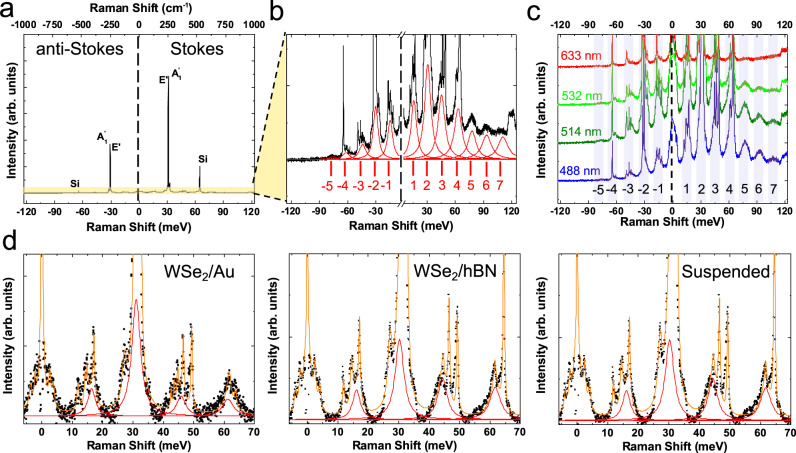
A typical RT Raman spectrum for 1L-WSe2 on SiO2/Si measured at 532 nm is shown in Fig. 1a. The degenerate in-plane, E, and out-of-plane, A1, modes of 1L-WSe243 dominate the spectrum at ~−250 cm−1 (−31 meV) and ~+250 cm−1 (+31 meV) in the AS and S range, while weaker Raman peaks are also observed between 90 cm−1 (11 meV) and 500 cm−1 (62 meV) (see Methods and Supplementary Note 1) as discussed in refs. 4446. Rescaling the intensity within the region marked in yellow in Fig. 1a reveals an underlying periodic pattern, Fig. 1b. Hereafter, for the energy scale we will use meV instead of cm−1. We fit all the peaks between −120 meV and +120 meV using Lorentzians, as shown in red in Fig. 1b. The fitting process is described in Methods. There are 7 S peaks and 5 AS at 295 K. The peak ~120 meV (~970 cm−1) originates from a combination of the Si substrate Γ1,Γ12,Γ25 phonons47. Although the energy separation between two consecutive peaks is constant, the intensity decreases as a function of energy with respect to the excitation energy (here fixed at 0). To exclude other contributions, such as thin-film interference effects48, we measure 1L-WSe2 transferred on Au, placed on top of few-layer (FL) (~10 nm) hBN and also suspended, Fig. 1d (see Methods and Supplementary Note 1 for optical microscope images and PL characterisation). The intensity of the hot PL is comparable among the same steps of the cascade, and the position of the peaks is the same. Therefore, the cascade is linked to intrinsic relaxation mechanisms of 1L-WSe2, not to substrate-induced interference. Henceforth we will focus on 1L-WSe2 on SiO2/Si.

Raman and hot PL spectra of 1L-WSe2.
Fig. 1

Raman and hot PL spectra of 1L-WSe2.

a Emission and scattering spectrum of 1L-WSe2 at 295K as a function of energy shift with respect to the excitation laser (532 nm~2.33eV). The degenerate in-plane (E) and out-of-plane (A1) Raman mode ~250 cm−1 43, as well as the Si Raman peak ~521 cm−1 47, are prominent in both S and AS. b Magnified portion of the spectrum in yellow in a. This reveals 7 periodic S peaks and 5 AS. Their intensity decreases as a function of the energy shift for both S and AS. c Raman spectra of 1L-WSe2 on SiO2/Si at 488, 514, 532, 633 nm and 295 K, shifted vertically for clarity. d Raman spectra of 1L-WSe2 on different substrates (Au, hBN and suspended) at 295K and 514 nm excitation. Black points: experimental data. Red lines: fitted cascades. Orange line: sum of fitted Lorentzians.

To exclude the possibility that our laser is in resonance with a specific transition, we perform variable excitation wavelength experiments at 295K. Figure 1c plots the spectra measured at 488 nm (~2.54 eV), 514 nm (~2.41 eV), 532 nm (~2.33 eV) and 633 nm (~1.96 eV). We observe the same high-order features with identical energy separations in both S and AS. All these excitation energies lie above the free-carrier gap of 1L-WSe2 ~ 1.89 eV4951. By comparing results for 1L-WSe2 on different substrates and for different excitation energies, we deduce that phonon-assisted hot PL is the dominant mechanism, whereas contributions from other excitations, such as plasmons52, are negligible, otherwise intensity and/or energy variations would be expected between Au and SiO2/Si, hBN, suspended cases.

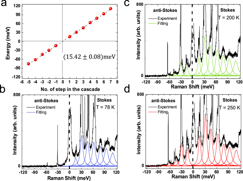
Figure 2a plots the energy offset with respect to the excitation laser (here 532 nm) of each emission feature as a function of the number of steps in the cascade at 295 K. Applying a linear fit, we extract ~15.42 ± 0.08 meV, regardless of substrate and excitation energy. This periodic modulation of the detected light intensity suggests that the scattering of photoexcited carriers is dominated by one prominent phonon mode. Since we excite above the free-carrier gap of 1L-WSe249, the intermediate states of the transitions are real. The e-h pair representation is in Fig. 3a.

Energy separation and T dependence.
Fig. 2

Energy separation and T dependence.

a Emission energies as a function of number of steps in the cascade, extracted from the RT spectrum in Fig. 1b. The dashed black line is a linear fit, giving a step energy ~15.42 ± 0.08meV. bd 532 nm Hot PL spectra of 1L-WSe2 at b 78 K, c 200 K, d 250 K.

Comparison between experiments and theory.
Fig. 3

Comparison between experiments and theory.

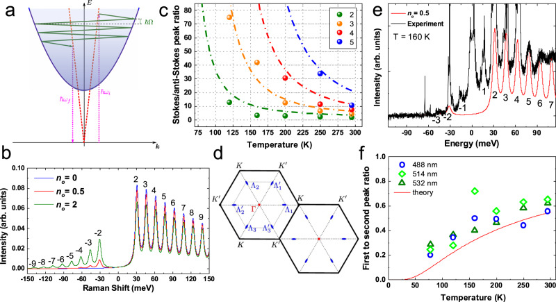
a Scheme of phonon-assisted hot PL. The incident, ωi, and outgoing, ωf, photons are shown by dotted magenta vertical arrows. The phonons participating in the cascade are indicated by the green arrows. The eh pair dispersion curve is the blue parabola. The light cone is shown by red dashed lines. b Calculated S/AS spectra at different T. c IS/IAS for different numbers of cascade steps as a function of T. Filled circles are experimental data at 532 nm. The fit with Eq. (9) is indicated by dot-dashed lines. d Extended BZ of 1L-WSe2. Corresponding valleys are marked as Γ, K, K and Λi, Λi (i = 1, …, 3). e Experimental data at 160K (black line) compared to the calculated spectrum from Eq. (2) for no = 0.5. f Ratio of measured intensities of j = 1 to j = 2 peaks and corresponding fit with Eq. (10).

The lattice T could affect the peaks intensity, as phonon occupation increases with T53,54. We thus perform T dependent measurements from 78 to 295 K, while keeping the excitation power constant ~26 μW. No emission of AS features is observed at 78 K, Fig. 2b, with the exception of two sharp lines ~−30 and ~−60 meV, originating from 1L-WSe2 and Si Raman modes, respectively. The hot PL peaks are seen at 200 K, Fig. 2c, and a further increase in intensity is observed at 250 K, Fig. 2d. Additional measurements at 120, 160, and 295 K are performed and used in the fits in Fig. 3c. Thermal effects are expected to modify the phonon energies55. However, in the 78–298 K range we do not observe any measurable shifts in the position of the hot PL peaks, because the shifts induced by acoustic phonons are smaller compared to our experimental error, as discussed in Methods.

Discussion

At low T (78 K), phonon absorption processes are suppressed because of the insufficient lattice thermal energy53. Optical excitation results in free e-h pair formation56,57 or virtual formation of an exciton with small in-plane wavevector (k ≲ ωi/c with ωi the excitation laser frequency)1. With the subsequent phonon emission, the e-h pair reaches a real final state (blue parabola in Fig. 3a), for which radiative recombination is forbidden by momentum conservation19. This triggers a cascade relaxation process36, whereby at each step a phonon is emitted (or absorbed for a T whereby the thermal energy is equal or higher than the phonon one energy)19. If the interaction with one phonon mode with energy Ω dominates overall other inelastic scattering processes, the exciton loses energy by integer multiples of Ω19,36. After emission of several (≥2) phonons, the exciton recombines and emits a photon with frequency ωf in a two-step process via an intermediate state with a small (k ≲ ωi/c) wavevector, for which radiative recombination is momentum allowed. Thus, we have secondary emission or scattering of light with S shift ωi − ωf = jΩ, where j = 2, 3, …., while j = ±1 are impossible as we scatter out of the light cone (i.e. the region of small wavevectors) with the first event. At finite T, in addition to phonon emission, absorption also comes into play, and AS emission is observed at ωf − ωi = jΩ.

Multiphonon processes that do not involve real states require higher order exciton–phonon interactions58, and are therefore less probable. In contrast, the process in Fig. 1c is resonant, since excitation in the free-carrier gap means that all intermediate states are real. This allows us to describe the phonon emission cascade via the kinetic equation for the exciton distribution function f(ε), where ε is the exciton energy, as derived in Supplementary Notes 2, 3. Since the energy of the exciton changes in each scattering event by ±Ω, the distribution function can be written as:

where ε0 is the excitation energy, δ(ε) is the Dirac δ-distribution (phonon dispersion and damping result in the broadening of the δ-distribution, as detailed in Supplementary Notes 2, 3), fj describes the peaks intensity. At steady state (partial derivative with respect to time equals zero) these obey a set of coupled equations describing the interplay of in- and out-scattering processes:
where no=expΩ/kBT11 is the phonon mode occupancy at T, γo is the rate of the spontaneous phonon emission, γ=γo(2no+1)+γ, is the total damping rate of the exciton, which includes recombination and inelastic scattering processes γ. The last term in Eq. (2), gδj,0, describes the exciton generation at energy ε0, and is proportional to the exciton generation rate. Eq. (2) has the boundary conditions:
where K is the maximum number of steps in the cascade:
with E1 the energy of the exciton band bottom. Eq. (2) is derived assuming γo and γ independent of ε. This assumption is needed to get an analytical solution of Eq. (2), but can be relaxed (see Supplementary Notes 2, 3).

The general solution of Eq. (2) is:

where
and x+ > 1 and x < 1, A, B and C are the coefficients. For cascades with K ≫ 1 we can set B = 0 and:
In this model, the spectrum of the scattered light consists of peaks with I ∝ fj, and scattering cross-section:
Here σ0(ωi, ωf) is a smooth function of frequency, Γ is the phonon damping. This description is valid for peaks with ∣j∣ > 1, the prime at the summation denotes that the terms with j = 0, ±1 are excluded. Accordingly, the peaks with Raman shift ±Ω are suppressed. At no → 0 (limit of low T), x+ ≫ 1 and Ij with negative j (AS components) are negligible. At the same time, x → (γo/γ) and the S peak intensities, IS, scale as (γo/γ)j. This scaling is natural for cascade processes19,59,60, since the probability of phonon emission relative to all other inelastic processes is given by γo/γ, thus IS decays in geometric progression. At finite T, the AS peaks appear with IAS proportional to the thermal occupation of the phonon modes. Thus, the S/AS intensity ratio, IS/IAS, with j steps in the cascade, can be written as:
and corresponds to the ratio of phonon emission and absorption rate to the power of j.

The calculated I distribution and spectra at various T (corresponding to different no) are presented in Fig. 3b. Figure 3c plots IS/IAS as a function of T from Eq. (9). The experimental points collected from the fitted I of each step in the cascade at 532 nm excitation are displayed with circles. The absence of data at 78 K indicates no detection of IAS at this T. Applying Eq. (9) to the steps 2–5 in the cascade, with a phonon energy ~15.4 meV extracted from Fig. 2a, gives the dashed lines in Fig. 3c, in good agreement with experiments.

Our model captures the main experimental observations well. The periodic pattern of hot PL intensity is reproduced by the calculations, Fig. 3b, and IS/IAS closely follows Eqs. (9), Fig. 3c. There is good agreement between our data and the calculated spectra from Eq. (2). An example for no = 0.5 at 160 K is in Fig. 3e. In our model, the peaks with j = ±1 are absent because N ≥ 2 phonons are needed for the first step of the cascade process, as for Fig. 3a. However, Fig. 1 shows that j = ±1 peaks are smaller than j = ±2 ones, but still detectable. We consider IS(1)/IS(2) as plotted in Fig. 3f. The possible mechanisms of j = 1 peak formation are as follows. (i) Elastic disorder or acoustic phonon-induced scattering, which provides a transfer between states within the light cone and states at the dispersion. (ii) Combination of phonon emission and absorption, where the j = 1 peak appears as a result of two phonon emission, followed by one phonon absorption. In (i) IS(1)/IS(2) does not depend on T. In (ii):

strongly depends on T. This is indeed the case in our experiment, see Fig. 3f. This additional channel is also based on the interaction with the same phonon energy ~15 meV. Elastic processes could be the origin of a small offset between the experiment and the fitted curve.

To get a better understanding of the relaxation pathways, we consider different scattering mechanisms. Scattering within the same valley is not plausible, due to the mismatch of BZ centre phonon energies61. The energy ~15 meV could correspond to either Γ − K or Γ − Λ phonons. The phonon dispersion in 1L-WSe2 shows acoustic phonons with energies ~15 meV46,61. These have a flat dispersion, necessary to observe the high number of oscillations we report, and are compatible with the model in Fig. 3a.

Another option involves K-K scattering of e (h) or, equivalently, Γ-K scattering of excitons. This would result in intensity oscillations as a function of the step in the cascade, due to the suppression of the process ΓKKΓ compared to, Γ → K → Γ (see Supplementary Notes 4, 5). However, we do not observe intensity oscillations for different cascade steps in our spectra. As a result, we exclude this scenario. Therefore, the excitonic states in the Λ valleys play a role as intermediate states, Fig. 3d. The conduction band minima in these valleys are relatively close (~35 meV) to K, and play a crucial role in exciton formation and relaxation6265. In this case, h remain in K (or K), but e scatter to any of the 6 available Λ valleys, and then scatter between these Λ valleys, before going back to K (K). This can be described taking into account all pathways, as:

with arbitrary number of steps j (both odd and even). The matrix elements of the processes are similar. We do not observe any noticeable periodic emission for 1L-MoS2 and 1L-WS2. This supports our interpretation, as the phonon scattering mechanism is linked to the particular bandstructure of 1L-WSe262.

Similar oscillations can appear for free e and h36, see Supplementary Note 4. The basic description of the effect is similar to what we observe here, and our model can be extended to take into account e/h distribution functions. The spectra of scattered light and IS/IAS are similar to those calculated above. We cannot distinguish between exciton and the free-carrier cascades directly in our experiments. The excitonic description, however, seems straightforward due to enhanced (with respect to bulk materials) Coulomb effects in 1L-TMDs1.

In conclusion, we investigated the light scattered and emitted by 1L-WSe2 excited above the free-carrier gap. We detected a periodic modulation of phonon-assisted hot PL with a period ~15 meV both in S and AS. We measured the S and AS intensity evolution from 78 to 295 K. We explained these high-order processes using a cascade model where electrons (holes) make successive transitions between real states with a finite probability of radiative recombination at each step. The electron states in the Λ valleys are intermediate states for efficient exciton relaxation. Our findings provide fundamental understanding of the initial steps of exciton relaxation in 1L-WSe2, and can be used to design optoelectronic devices based on this material. Our approach can be extended also to other layered materials and their heterostructures, as well as to perovskites.

Methods

Raman and PL spectra fitting

Supplementary Fig. 1a–c presents optical microscopy images of representative samples: (a) 1L-WSe2 on Au and suspended 1L-WSe2; (b) 1L-WSe2 on SiO2/Si; (c) 1L-WSe2 on hBN. Representative PL spectra collected 295 K at 514 nm excitation are in Supplementary Fig. 1d, showing a peak ~1.65 eV related to the A-exciton resonance1,12. Supplementary Fig. 2a shows representative data fits. The spectrum, at 295 K for 532 nm excitation, is shown with black dots. Blue lorentzian functions are used to fit the Raman peaks (FWHM ~ 1–10 cm−1). The residual spectral weight is also fitted with Lorentzians and results into the broader (FWHM ~ 50–80 cm−1) peaks of the hot PL (red). A flat baseline is taken into account for the whole energy scale, since the background in the S spectral range increases due to the higher intensity of the S cascades compared to the AS ones. A fit is shown in Supplementary Fig. 2b. The Lorentzians overlap, creating an asymmetric broad background (indicated by yellow dashed lines in Supplementary Fig. 2b).

We now consider the thermally induced shift in the hot PL cascades of 1L-WSe2 in the 78–295 K range. We analyze Pos(E, A1), as shown in the normalized intensity spectra in Supplementary Fig. 2c. Pos(E, A1) red shift as a function of T, Supplementary Fig. 2d. Although the overall T dependence is not linear55, in the 78–295 K range we get:

where k is the slope. This corresponds to a shift of ~0.2 meV in the 78–295 K range. However, acoustic modes participate in the hot PL phonon cascades and their T dependence is weaker compared to optical phonons66. Thus ~0.2 meV is an upper limit of the expected shift of the hot PL cascades in this T range. The period ~15.42 ± 0.08 meV is quantified at 295 K by applying a linear fit in the position of the steps in the cascade in Fig. 2a, while the error bar corresponds to the standard error of the linear fit. This does not take into account other sources, such as the error in the dispersion of the grating, the fitting accuracy, etc, therefore the actual error bar is expected to be larger than 0.08 meV. Thus, although a shift of the order of less than one tenth of meV induced by acoustic phonons would be expected in this T range, it is very challenging to experimentally observe it in hot PL.

Peer review information: Nature Communications thanks the anonymous reviewer(s) for their contribution to the peer review of this work. Peer reviewer reports are available.
Publisher’s note: Springer Nature remains neutral with regard to jurisdictional claims in published maps and institutional affiliations.

Supplementary information

Supplementary information is available for this paper at 10.1038/s41467-020-20244-7.

Acknowledgements

We acknowledge funding from ANR 2D-vdW-Spin, ANR MagicValley, the Institut Universitaire de France, the RFBR and CNRS joint project 20-52-16303, EU Graphene Flagship, ERC Grants Hetero2D and GSYNCOR, EPSRC Grants EP/K01711X/1, EP/ K017144/1, EP/N010345/1, EP/L016087/1. G.W. acknowledges the support from the National Science Foundation of China Grant No. 11904019 and Beijing Natural Science Foundation Grant No. Z190006.

Author contributions

B.U., M.M.G., X.M., I.P. and A.C.F. conceived the project. I.P. and G.W. performed the experiments and acquired the data. I.P. analysed the results. I.P., E.M.A. and A.R.C. fabricated the samples. M.M.G. performed the theoretical studies. I.P., M.M.G., B.U., X.M. and A.C.F. wrote the manuscript. All authors discussed the results and commented on the manuscript at all stages.

Data availability

The data that support the findings of this study are available from the corresponding author upon request.

Competing interests

The authors declare no competing interests.

References

1. 

    Wang G, . Colloquium: excitons in atomically thin transition metal dichalcogenides. Rev. Mod. Phys.2018. 90: 021001 doi: 10.1103/RevModPhys.90.021001

2. 

    Cao T, . Valley-selective circular dichroism in MoS2.. Nat. Commun.2012. 3: 887 doi: 10.1038/ncomms1882

3. 

    Schaibley JR, . Valley depolarization dynamics and valley hall effect of excitons in monolayer and bilayer MoS2.. Nat. Rev. Mater.2016. 1: 16055 doi: 10.1038/natrevmats.2016.55

4. 

    Novoselov KS, Mishchenko A, Carvalho A, Castro Neto AH. 2d materials and van der waals heterostructures.. Science2016. 353: aac9439 doi: 10.1126/science.aac9439

5. 

    Mak KF, Shan J. Photonics and optoelectronics of 2d semiconductor transition metal dichalcogenides. Nat. Photonics2016. 10: 216-226 doi: 10.1038/nphoton.2015.282

6. 

    Unuchek D, . Room-temperature electrical control of exciton flux in a van der waals heterostructure. Nature2018. 560: 340 doi: 10.1038/s41586-018-0357-y

7. 

    Schneider C, Glazov MM, Korn T, Höfling S, Urbaszek B. Two-dimensional semiconductors in the regime of strong light-matter coupling. Nat. Commun.2018. 3: 2695 doi: 10.1038/s41467-018-04866-6

8. 

    Koperski M, . Optical properties of atomically thin transition metal dichalcogenides: observations and puzzles. Nanophotonics2017. 6: 1289-1308 doi: 10.1515/nanoph-2016-0165

9. 

    Dufferwiel S, . Valley-addressable polaritons in atomically thin semiconductors. Nat. Photonics2017. 11: 497 doi: 10.1038/nphoton.2017.125

10. 

    Scuri G, . Large excitonic reflectivity of monolayer mose2 encapsulated in hexagonal boron nitride. Phys. Rev. Lett.2018. 120: 037402 doi: 10.1103/PhysRevLett.120.037402

11. 

    Hong X, . Ultrafast charge transfer in atomically thin MoS2/WS2 heterostructures. Nat. Nanotechnol.2014. 9: 682 doi: 10.1038/nnano.2014.167

12. 

13. 

    Klimov VI, McBranch D, Leatherdale C, Bawendi M. Electron and hole relaxation pathways in semiconductor quantum dots. Phys. Rev. B1999. 60: 13740 doi: 10.1103/PhysRevB.60.13740

14. 

    Brida D, . Ultrafast collinear scattering and carrier multiplication in graphene. Nat. Commun.2013. 4: 1-9 doi: 10.1038/ncomms2987

15. 

    Kozawa D, . Photocarrier relaxation pathway in two-dimensional semiconducting transition metal dichalcogenides. Nat. Commun.2014. 5: 1-7 doi: 10.1038/ncomms5543

16. 

    Song Y, Dery H. Transport theory of monolayer transition-metal dichalcogenides through symmetry. Phys. Rev. Lett.2013. 111: 026601 doi: 10.1103/PhysRevLett.111.026601

17. 

    Glazov M. Quantum interference effect on exciton transport in monolayer semiconductors. Phys. Rev. Lett.2020. 124: 166802 doi: 10.1103/PhysRevLett.124.166802

18. 

Balkan, N. Hot Electrons in Semiconductors: Physics and Devices (Oxford University Press on Demand, 1998).

19. 

Peter, Y. & Cardona, M. Fundamentals of Semiconductors: Physics and Materials Properties (Springer Science & Business Media, 2010).

20. 

    Leite R, Scott J, Damen T. Multiple-phonon resonant raman scattering in CdS.. Phys. Rev. Lett.1969. 22: 780 doi: 10.1103/PhysRevLett.22.780

21. 

    Klein MV, Porto S. Multiple-phonon-resonance raman effect in CdS.. Phys. Rev. Lett.1969. 22: 782 doi: 10.1103/PhysRevLett.22.782

22. 

    Gross E, Permogorov S, Morozenko Y, Kharlamov B. Hot-exciton luminescence in CdSe crystals.. Phys. Status Solidi (b)1973. 59: 551-560 doi: 10.1002/pssb.2220590222

23. 

    Cerqueira M, . Resonant raman scattering in ZnO: Mn and ZnO: Mn: Al thin films grown by RF sputtering. J. Phys. Condens. Matter2011. 23: 334205 doi: 10.1088/0953-8984/23/33/334205

24. 

    Ursaki V, . Multiphonon resonant raman scattering in ZnO crystals and nanostructured layers. Phys. Rev. B2004. 70: 155204 doi: 10.1103/PhysRevB.70.155204

25. 

    Kumar B, Gong H, Chow SY, Tripathy S, Hua Y. Photoluminescence and multiphonon resonant raman scattering in low-temperature grown ZnO nanostructures. Appl. Phys. Lett.2006. 89: 071922 doi: 10.1063/1.2336997

26. 

    Vincent R, . Raman scattering in Me-doped ZnO nanorods (Me = Mn, Co, Cu and Ni) prepared by thermal diffusion. Nanotechnology2008. 19: 475702 doi: 10.1088/0957-4484/19/47/475702

27. 

    Sun W, Chua S, Wang L, Zhang X. Outgoing multiphonon resonant raman scattering and luminescence in Be-and C-implanted GaN. J. Appl. Phys.2002. 91: 4917-4921 doi: 10.1063/1.1455682

28. 

    Gołasa K, . Multiphonon resonant raman scattering in MoS2.. Appl. Phys. Lett.2014. 104: 092106 doi: 10.1063/1.4867502

29. 

    Robert C, . Exciton radiative lifetime in transition metal dichalcogenide monolayers. Phys. Rev. B2016. 93: 205423 doi: 10.1103/PhysRevB.93.205423

30. 

    Manca M, . Enabling valley selective exciton scattering in monolayer WSe2 through upconversion. Nat. Commun.2017. 8: 14927 doi: 10.1038/ncomms14927

31. 

    Han B, . Exciton states in monolayer MoSe2 and MoTe2 probed by upconversion spectroscopy. Phys. Rev. X2018. 8: 031073

32. 

    Brem S, Selig M, Berghaeuser G, Malic E. Exciton relaxation cascade in two-dimensional transition metal dichalcogenides. Sci. Rep.2018. 8: 1-8 doi: 10.1038/s41598-018-25906-7

33. 

    Kash J, Tsang J, Hvam J. Subpicosecond time-resolved raman spectroscopy of LO phonons in GaAs.. Phys. Rev. Lett.1985. 54: 2151 doi: 10.1103/PhysRevLett.54.2151

34. 

    Koppens F, . Photodetectors based on graphene, other two-dimensional materials and hybrid systems. Nat. Nanotechnol.2014. 9: 780-793 doi: 10.1038/nnano.2014.215

35. 

    Reeves L, Wang Y, Krauss TF. 2d material microcavity light emitters: to lase or not to lase?. Adv. Optical Mater.2018. 6: 1800272 doi: 10.1002/adom.201800272

36. 

37. 

    Zhao D, . Monitoring electron–phonon interactions in lead halide perovskites using time-resolved THz spectroscopy. ACS Nano2019. 13: 8826-8835 doi: 10.1021/acsnano.9b02049

38. 

    Yang J, . Acoustic-optical phonon up-conversion and hot-phonon bottleneck in lead-halide perovskites. Nat. Commun.2017. 8: 1-9 doi: 10.1038/s41467-016-0009-6

39. 

    Novoselov KS, . Two-dimensional atomic crystals. Proc. Natl Acad. Sci. USA2005. 102: 10451-10453 doi: 10.1073/pnas.0502848102

40. 

    Casiraghi C, . Rayleigh imaging of graphene and graphene layers. Nano Lett.2007. 7: 2711-2717 doi: 10.1021/nl071168m

41. 

42. 

    Orchin GJ, . Niobium diselenide superconducting photodetectors. Appl. Phys. Lett.2019. 114: 251103 doi: 10.1063/1.5097389

43. 

    Tonndorf P, . Photoluminescence emission and raman response of monolayer MoS2, MoSe2, and WSe2. Opt. express2013. 21: 4908-4916 doi: 10.1364/OE.21.004908

44. 

    Zhao W, . Lattice dynamics in mono-and few-layer sheets of WS2 and WSe2.. Nanoscale2013. 5: 9677-9683 doi: 10.1039/c3nr03052k

45. 

    Li H, . Mechanical exfoliation and characterization of single-and few-layer nanosheets of WSe2, TaS2, and TaSe2.. Small2013. 9: 1974-1981 doi: 10.1002/smll.201202919

46. 

    Jin Z, Li X, Mullen JT, Kim KW. Intrinsic transport properties of electrons and holes in monolayer transition-metal dichalcogenides. Phys. Rev. B2014. 90: 045422 doi: 10.1103/PhysRevB.90.045422

47. 

    Temple PA, Hathaway C. Multiphonon raman spectrum of silicon. Phys. Rev. B1973. 7: 3685 doi: 10.1103/PhysRevB.7.3685

48. 

49. 

    Goryca M, . Revealing exciton masses and dielectric properties of monolayer semiconductors with high magnetic fields. Nat. Commun.2019. 10: 1-12 doi: 10.1038/s41467-019-12180-y

50. 

    Wang G, . Giant enhancement of the optical second-harmonic emission of WSe2 monolayers by laser excitation at exciton resonances. Phys. Rev. Lett.2015. 114: 097403 doi: 10.1103/PhysRevLett.114.097403

51. 

52. 

    Van Tuan D, Scharf B, Žutić I, Dery H. Marrying excitons and plasmons in monolayer transition-metal dichalcogenides. Phys. Rev. X2017. 7: 041040

53. 

    Jellison Jr G, Lowndes D, Wood R. Importance of temperature-dependent optical properties for raman-temperature measurements for silicon. Phys. Rev. B1983. 28: 3272 doi: 10.1103/PhysRevB.28.3272

54. 

    Kip BJ, Meier RJ. Determination of the local temperature at a sample during raman experiments using stokes and anti-stokes raman bands. Appl. Spectrosc.1990. 44: 707-711 doi: 10.1366/0003702904087325

55. 

    Li Z, . Temperature-dependent raman spectroscopy studies of 1–5-layer WSe2. Nano Res.2020. 13: 591-595 doi: 10.1007/s12274-020-2669-0

56. 

    Steinleitner P, . Direct observation of ultrafast exciton formation in a monolayer of WSe2.. Nano Lett.2017. 17: 1455-1460 doi: 10.1021/acs.nanolett.6b04422

57. 

    Trovatello C, . The ultrafast onset of exciton formation in 2d semiconductors.. Nat. Commun.2020. 11: 5277 doi: 10.1038/s41467-020-18835-5

58. 

    Shree S, . Observation of exciton-phonon coupling in MoSe2 monolayers. Phys. Rev. B2018. 98: 035302 doi: 10.1103/PhysRevB.98.035302

59. 

    Ivchenko E, Lang I, ST P. Theory of resonance secondary radiation emitted by semiconductors. Phys. Solid State1977. 19: 1610

60. 

    Goltsev A, Lang I, Pavlov S, Bryzhina M. Multiphonon resonance raman scattering and spatial distribution of electrons and holes. J. Phys. C Solid State Phys.1983. 16: 4221 doi: 10.1088/0022-3719/16/21/023

61. 

    He M, . Valley phonons and exciton complexes in a monolayer semiconductor. Nat. Commun.2020. 11: 618 doi: 10.1038/s41467-020-14472-0

62. 

    Kormanyos A, . k.p theory for two-dimensional transition metal dichalcogenide semiconductors. 2D Mater.2015. 2: 022001 doi: 10.1088/2053-1583/2/2/022001

63. 

    Selig M, . Dark and bright exciton formation, thermalization, and photoluminescence in monolayer transition metal dichalcogenides. 2D Mater.2018. 5: 035017 doi: 10.1088/2053-1583/aabea3

64. 

    Madéo J, . Directly visualizing the momentum-forbidden dark excitons and their dynamics in atomically thin semiconductors.. Science2020. 370: 1199-1204 doi: 10.1126/science.aba1029

65. 

    Rosati R, . Temporal evolution of low-temperature phonon sidebands in WSe2 monolayers.. ACS Photonics2020. 7: 2756-2764 doi: 10.1021/acsphotonics.0c00866

66. 

    Mobaraki A, Sevik C, Yapicioglu H, Cakir D, Gülseren O. Temperature-dependent phonon spectrum of transition metal dichalcogenides calculated from the spectral energy density: Lattice thermal conductivity as an application. Phys. Rev. B2019. 100: 035402 doi: 10.1103/PhysRevB.100.035402