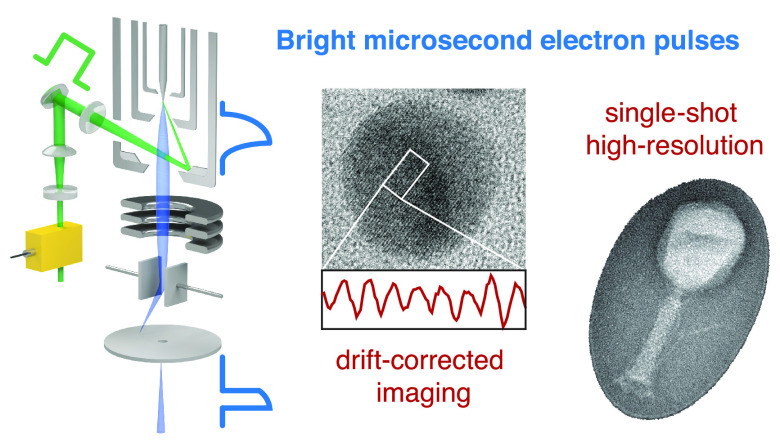
 Atomic-Resolution
Imaging of Fast Nanoscale Dynamics
with Bright Microsecond Electron Pulses
Atomic-Resolution
Imaging of Fast Nanoscale Dynamics
with Bright Microsecond Electron Pulses
Nano Letters


- Altmetric
Atomic-resolution electron microscopy is a crucial tool to elucidate the structure of matter. Recently, fast electron cameras have added the time domain to high-resolution imaging, allowing static images to be acquired as movies from which sample drift can later be removed computationally and enabling real-time observations of atomic-scale dynamics on the millisecond time scale. Even higher time resolution can be achieved with short electron pulses, yet their potential for atomic-resolution imaging remains unexplored. Here, we generate high-brightness microsecond electron pulses from a Schottky emitter whose current we briefly drive to near its limit. We demonstrate that drift-corrected imaging with such pulses can achieve atomic resolution in the presence of much larger amounts of drift than with a continuous electron beam. Moreover, such pulses enable atomic-resolution observations on the microsecond time scale, which we employ to elucidate the crystallization pathways of individual metal nanoparticles as well as the high-temperature transformation of perovskite nanocrystals.
Specimen drift presents a fundamental challenge for high-resolution imaging, particularly for in situ experiments where rapid changes of the sample temperature or some other variable induce large amounts of drift.1 But even the exposure of the sample to the electron beam itself may cause beam-induced sample motion. Fast electron cameras have alleviated this problem, allowing one to record micrographs as movies, so that drift can be removed computationally by aligning the movie frames to each other before adding them up.2 Such dose-fractionated imaging has, for example, become crucial in cryo-electron microscopy.2 Nevertheless, if the amount of drift present in a movie frame exceeds the target resolution, it has to be discarded. This is frequently the case for the first frames of cryo-electron micrographs, which are particularly affected by beam-induced drift.2
Fast electron cameras are also used to observe processes in real time that are purposefully induced in situ, for example, with electrical impulses, through mechanical deformation, heating, or laser irradiation of the sample.3−7 The time resolution of such in situ experiments is ultimately limited by the frame rate of the electron camera, as is the amount of drift that can be removed with dose-fractionated imaging. A vastly higher time resolution can be obtained by imaging with short electron pulses, a principle that is employed in time-resolved electron microscopy to capture processes down to the femtosecond time scale.8−12 However, atomic-resolution imaging with short electron pulses has largely remained elusive. For example, while it has been proposed that it should be possible to image the dynamics of proteins at atomic resolution with a single electron pulse,13,14 the spatial resolution currently achieved in such single-shot experiments is several nanometers.14 The challenge here lies in the creation of electron pulses that are coherent enough to enable atomic-resolution imaging but also contain a sufficiently large number of electrons to be able to capture the image information in a single shot, or a small number of pulses if the image is recorded stroboscopically.
Results and Discussion
Generation of High-Brightness Electron Pulses
Here, we demonstrate that such intense, high-brightness electron pulses can be generated by temporarily boosting the emission current of a Schottky emitter to near its limit15 and chopping the electron beam into pulses with an electrostatic deflector. As illustrated in Figure 1a,b, we irradiate the emitter tip with a microsecond laser pulse, which is generated by chopping the output of a continuous laser beam (532 nm) with an acousto-optic modulator. A mirror embedded within the emitter assembly directs the laser beam at the tip of the Schottky emitter (Figure 1a), where it is focused to a spot size of 17 μm fwhm. As shown in Figure 1c, illumination with a 100 μs laser pulse of 0.44 W (green curve) temporarily boosts the probe current (blue) from 60 nA to a peak of 200 nA. Under these conditions, the emitter tip reaches an estimated temperature of about 2500 K, significantly above the maximum safe operating temperature of 1850 K (ref (16)), which briefly increases the emission current to an extreme value15 that can otherwise not be sustained without damaging the emitter.16,17

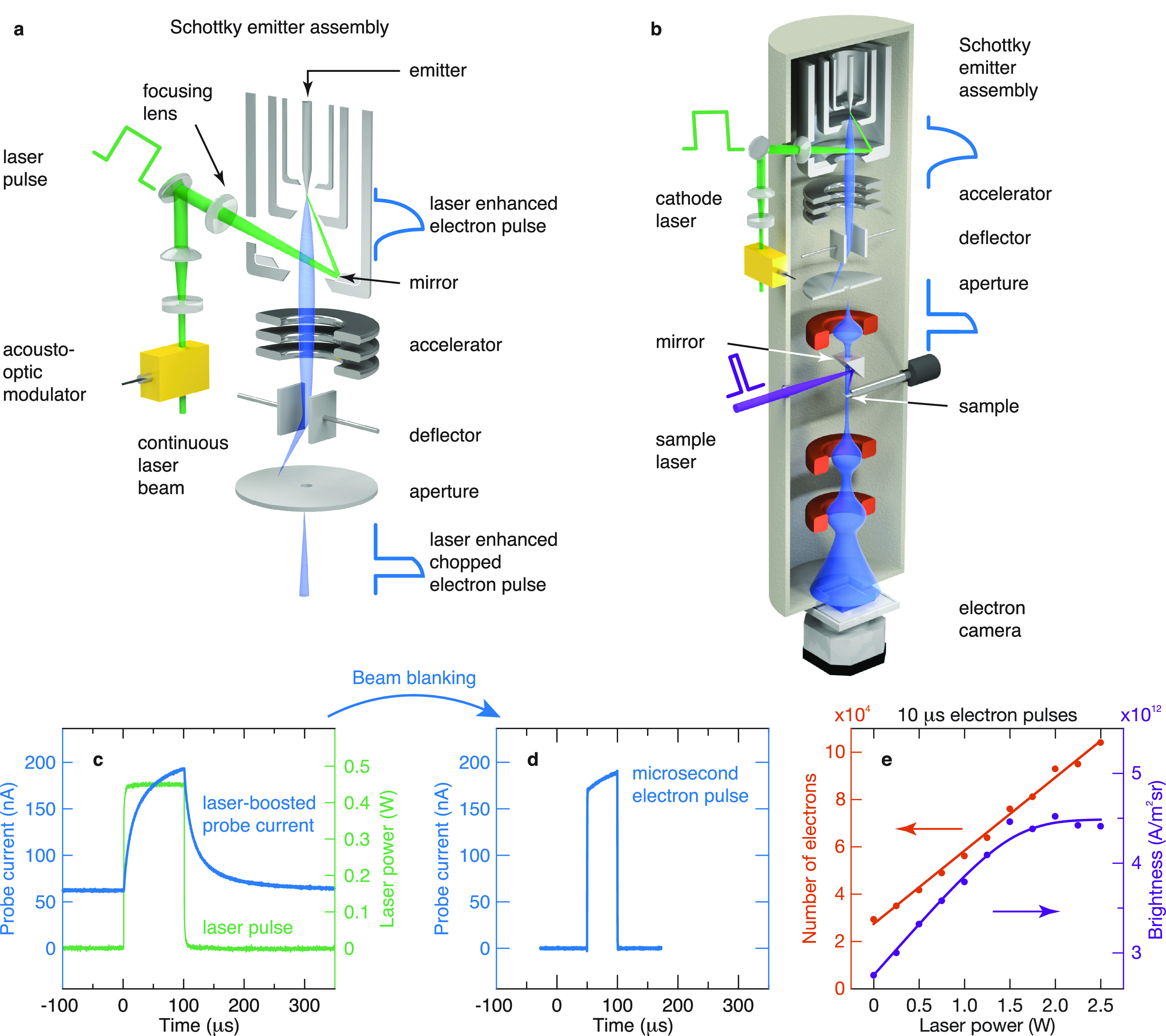
Generation of intense microsecond electron pulses of high brightness. (a) A microsecond laser pulse heats the tip of a Schottky emitter to boost emission, while an electrostatic deflector chops the electron beam into microsecond pulses. (b) Illustration of the time-resolved electron microscope. Dynamics of the sample are initiated with a short laser pulse and probed with a microsecond electron pulse. (c) The probe current (blue) is boosted when the emitter tip is heated with a microsecond laser pulse (green). (d) An intense microsecond electron pulse is obtained by chopping the boosted electron beam with the deflector. (e) Number of electrons in a 10 μs electron pulse (red) and instantaneous brightness (purple) as a function of laser power. The solid lines serve as a guide for the eye.
As illustrated in Figure 1a, the laser-boosted electron beam is chopped into pulses by means of an electrostatic deflector that is placed after the accelerator of the gun and that sweeps the beam over a small aperture. This allows us to generate electron pulses of microsecond duration, as demonstrated in Figure 1d, and even pulses as short as 100 ns. These laser-boosted pulses are not only intense but also possess a high instantaneous brightness, which is crucial for high-resolution imaging.18Figure 1e shows that the brightness initially increases linearly with laser power but levels off as electron–electron interactions in the beam become more frequent.17,19 At the highest laser power, it reaches 1.7 times the value without boost laser, while the number of electrons per pulse has almost quadrupled (see also Figure S1). As illustrated in Figure 1b, the electron gun and deflector assembly are mounted on a JEOL 2010F transmission electron microscope that we have modified for time-resolved experiments.19 Dynamics of the specimen are initiated in situ with pulses from a 405 nm diode laser that is directed at the sample with a mirror mounted above the upper pole piece of the objective lens (34 μm spot size in the sample plane). A laser-boosted electron pulse is then used to capture a snapshot of the dynamics with the electron camera.
Drift Corrected Imaging
We first demonstrate the potential of our laser boosted electron pulses to improve the resolution of drift-corrected imaging by delivering the electron dose per movie frame in a short burst instead of spreading it out evenly, so that even larger amounts of drift can be outrun. Figure 2a displays a micrograph of a 15 nm diameter gold particle on an amorphous carbon substrate (full frame image in Figure S2) acquired with a continuous electron beam in the presence of substantial drift. In order to induce a well-defined amount of drift, the sample was irradiated with a continuous laser beam whose power was increased linearly during acquisition. The image was recorded as a movie of 10 frames of 41 ms duration each, corresponding to the fastest frame rate of our camera at full frame read-out (410 ms total exposure time), and subsequently drift corrected with cisTEM.20 The drift path obtained in the alignment procedure reveals that the sample drifted with a speed of 9 nm/s, corresponding to 3.5 Å per frame (Figure 2b), which explains the blurry appearance of the image. In contrast, if we acquire each movie frame with a laser-boosted electron pulse of 480 μs duration, the image resolution is markedly improved, as shown in Figure 2c (same total electron dose and drift, see Figure 2d). The gold nanoparticle now exhibits lattice fringes, which are also evident in the intensity profile (inset) of the area marked with a rectangle and which are entirely absent in the image recorded with a continuous electron beam.
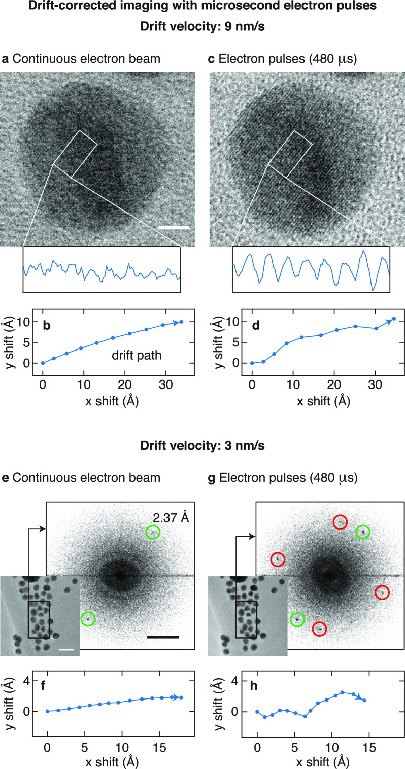
Drift-corrected imaging with microsecond electron pulses. (a,c) Drift-corrected images of a gold nanoparticle (from the full frame micrographs in Figure S2), recorded with a continuous electron beam (a) and with 480 μs electron pulses (c) in the presence of a drift velocity of 9 nm/s. When imaged with electron pulses, the particle exhibits lattice fringes, as evident in the intensity profile of the region marked with a white rectangle. Scale bar, 3 nm. (b,d) Drift path of the sample during acquisition of the images in (a) and (c), respectively. (e,g) Drift-corrected images of an ensemble of gold nanoparticles, recorded with a continuous electron beam (e) and with 480 μs electron pulses (g) in the presence of a drift velocity of 3 nm/s. Diffractograms of the area marked with a black rectangle reveal several reflections of the gold nanoparticles (2.37 Å) that are present in the image recorded with a pulsed electron beam but absent when recorded with a continuous beam. Scale bars, 30 nm and 2.5 nm–1. (f,h) Drift path of the sample during acquisition of the images in (e) and (g), respectively.
Imaging with intense microsecond electron pulses affords an improved resolution even at lower drift rates, similar, for example, to those encountered in the first movie frames of cryo-electron micrographs.2 When we image an ensemble of gold nanoparticles on lacey carbon with 14 frames of 41 ms duration (Figure 2e,g,) while the sample drifts with a speed of 3 nm/s, corresponding to 1.4 Å per frame (Figure 2f,h), diffractograms of the area marked with a rectangle reveal several reflections (red circles, 2.37 Å) for the micrograph recorded with pulsed illumination (Figure 2g) that are absent or much weaker with a continuous beam (Figure 2e). As we demonstrate in Figure S3, imaging with electron pulses is also advantageous if drift is not induced by an external stimulus but instead results from the exposure of the sample to the electron beam itself.
Single-Shot Imaging
Next, we demonstrate the ability of our intense electron pulses to capture microsecond single-shot images with atomic resolution. Figure 3a displays a 15 nm diameter gold nanoparticle that was imaged with 15 laser-boosted electron pulses of 10 μs duration. In order to obtain the highest electron dose, the electron beam is almost fully converged to an area barely larger than the object. Even under such extreme imaging conditions, the particle features lattice fringes, which are also evident in the intensity profile of the area marked with a rectangle as well as the diffractogram of the image (insets). An individual single-shot micrograph is shown in Figure 3b. Even though it is noisier, it demonstrates that atomic-resolution information can be captured with just a single 10 μs electron pulse. Another example is presented in Figure 3c, which shows a micrograph of negatively stained Bacteriophage T4 (ref (21)), imaged with 20 pulses of 50 μs duration. An intensity profile and diffractogram (insets) of the phage tail (white bracket) reveal the characteristic 39 Å spacing of the tail sheath proteins,21 which are also evident in an individual single-shot image (Figure 3d). We conclude that pulses of tens of microseconds offer sufficient contrast for single-shot imaging while being coherent enough to achieve atomic resolution.
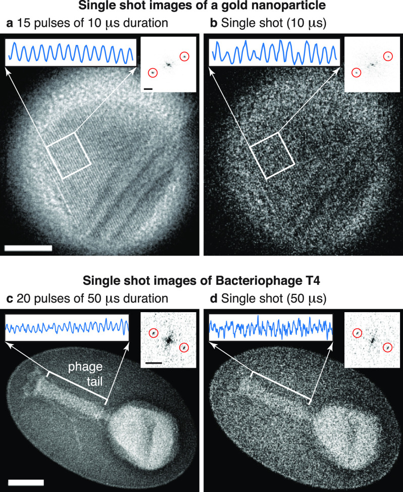
Atomic-resolution single-shot imaging. (a,b) Single-shot images of a gold nanoparticle recorded with 10 μs electron pulses. In (a), 15 pulses of 10 μs duration are averaged, while (b) shows an image recorded with an individual 10 μs pulse. Line profiles of the area marked with a rectangle (left insets) and diffractograms of the particle (right insets) reveal lattice fringes with a spacing of 2.35 Å. Scale bars, 5 nm, as well as 2 nm–1 in the inset. (c,d) Single-shot images of negatively stained Bacteriophage T4 recorded with 50 μs electron pulses. In (c), 20 pulses of 50 μs duration are averaged, while (d) shows an image recorded with an individual 50 μs pulse. Intensity profiles (left insets) and diffractograms (right insets) of the area corresponding to the phage tail (marked with a white bracket) reveal the spacing of the tail sheath proteins of 39.0 Å. Scale bars, 50 nm, as well as 0.25 nm–1 in the inset.
Single-Shot Imaging of Nanoscale Dynamics
Finally, we demonstrate that our laser-boosted electron pulses allow us to capture fast, atomic-scale transformations in a single shot. We illustrate this by studying the competing crystallization pathways of an individual lead nanoparticle (Figure 4a, circle), which we melt in situ with a laser pulse (500 μs, 1 mW) before letting it rapidly crystallize in the presence of an adjacent CsPbBr3 perovskite nanocrystal (rectangle) that provides a nucleation seed. A single-shot image recorded during the laser pulse (Figure 4b) establishes that the lead particle is completely melted, while the perovskite remains crystalline (see also the diffractograms of the particles in the insets). Subsequently, the lead particle crystallizes in a new configuration with several crystalline domains (Figure 4c).
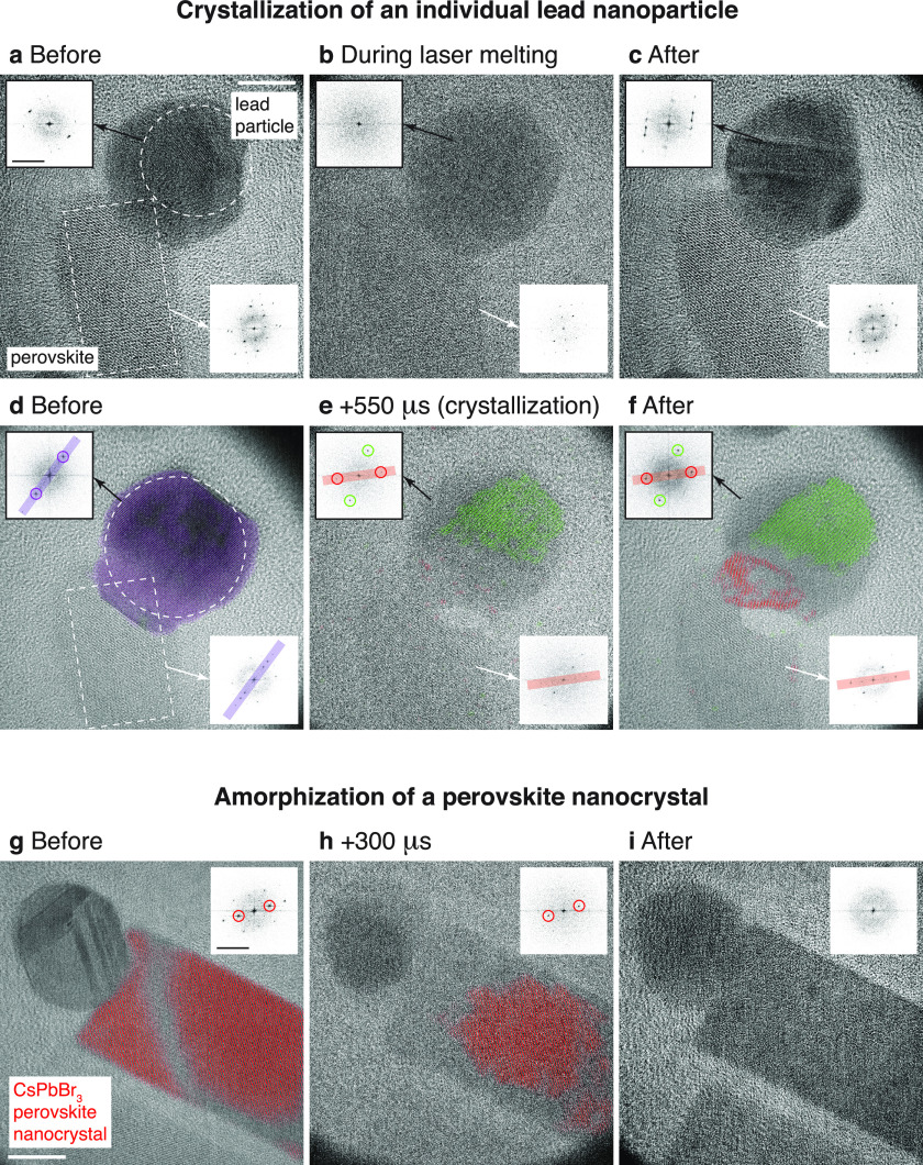
Single-shot imaging of atomic-scale transformations of nanoparticles. (a–f) Competing crystallization pathways of an individual lead nanoparticle. The lead particle (marked with circle in a) is melted in situ with a laser pulse (500 μs, 1 mW) with the adjacent perovskite nanocrystal (rectangle) providing a nucleation seed for the subsequent crystallization process. A snapshot recorded during laser irradiation (b) reveals that the lead particle is completely melted, while the perovskite remains crystalline (100 μs electron pulse, 200 μs before the end of the laser pulse). After the laser pulse, the lead particle cools and recrystallizes in a different configuration (c). The insets show diffractograms of both particles. (d–f) The melting and recrystallization process is repeated (500 μs laser pulse, 2 mW), creating another configuration of the lead particle with several crystalline domains (f). Colored overlays highlight domains of different orientation and are obtained by Fourier filtering the images with the reflections selected that are circled in the diffractograms in the insets. A snapshot taken during the crystallization process (e, 550 μs after the end of the laser pulse) reveals that the formation of the domain highlighted in green precedes that of the domain highlighted in red. Colored bars in the diffractograms highlight sets of reflections of the lead particle and the perovskite that are parallel to each other, suggesting that the perovskite acted as a nucleation seed in the crystallization process. Scale bars, 10 nm and 5 nm–1. (g–i) Amorphization of a perovskite nanocrystal under laser heating. The CsPbBr3 nanocrystal in panel g is rendered amorphous after illumination with a 500 μs laser pulse of 1 mW power (i), as evident from the diffractogram of the crystal in the inset. A snapshot recorded after 300 μs of laser irradiation (h) reveals that amorphization is initiated at the crystal boundaries (100 μs electron pulse). The red overlay highlights crystalline domains and is obtained by Fourier filtering the images with the reflections selected that are circled in the diffractogram in the inset. Scale bars, 10 nm and 5 nm–1.
When we repeat the crystallization process, different configurations are randomly obtained. Frequently, however, the perovskite nanocrystal appears to act as a nucleation seed (Figure S4) creating configurations such as the one in Figure 4d in which the lattice fringes of the lead particle are parallel to a set of planes of the perovskite crystal. This is also evident in the diffractograms, where the corresponding sets of reflections of both particles fall onto the same line (highlighted with purple bars). The lead particle has formed a single-crystal, as evident from the purple overlay highlighting areas of the same crystal orientation that was obtained by Fourier filtering with the reflections selected that are circled in the diffractogram. Melting and recrystallization creates yet another configuration (Figure 4f), which appears to result from the competition of different crystallization pathways. While the lattice fringes visible in the top (green) are randomly oriented, those in the bottom (red) are aligned with another set of lattice planes of the adjacent perovskite crystal (red bars in the diffractograms). A snapshot of the crystallization process yields insights into the crystallization trajectory (Figure 4e). Surprisingly, formation of the randomly oriented domain (green) precedes that of the heterogeneously nucleated domain (red), which appears to be just forming in the single-shot image. Such real-time observations promise to elucidate a range of phenomena that have so far only been studied theoretically for rapidly crystallizing metal nanoparticles, such as the cross-nucleation of polymorphs22 or the fate of crystallization seeds during crystal growth.23
As another example, we study the structural transformations that CsPbBr3 perovskite nanocrystals24,25 undergo at elevated temperatures. The perovskite nanocrystal in Figure 4g features a single crystalline domain highlighted in red. Heating the crystal with a 500 μs laser pulse (1 mW) renders it amorphous (Figure 4i), a process that is known to be associated with the degradation of the performance of perovskite nanocrystals in optoelectronic applications and that hinders their use in high-power devices.26 A snapshot taken during laser irradiation provides a subparticle picture of the mechanism involved, revealing that amorphization is initiated at the crystal boundaries and propagates inward (Figure 4h). We estimate that the amorphous domain expands with a speed of 35 nm/ms along the long axis of the crystal and with 5–12 nm/ms along its short axis. These observations suggest that interfaces play an important role in the high-temperature amorphization of perovskite nanocrystals and that their modification may provide a means to improve temperature stability.
Conclusion
In conclusion, we demonstrate both static and dynamic atomic-resolution imaging with intense, high-brightness electron pulses from a field emitter. We show that such electron pulses enable high-resolution imaging in the presence of large amounts of drift. For example, if 0.2 Å drift per frame are acceptable, then even a staggering drift rate of 40 nm/s can be tolerated if one images with 500 μs electron pulses, as we have done here. This particularly stands to benefit the field of in situ electron microscopy, where drift presents a fundamental challenge1 but may also be useful for any kind of high-resolution imaging affected by beam induced drift, such as cryo-electron microscopy. Atomic-resolution single-shot imaging with microsecond time resolution will enable the study of a wide range of irreversible atomic-scale processes. Of particular interest are the dynamics of proteins whose relevant motions frequently occur on the microsecond to millisecond time scale.27 Our experiments suggest that single-shot imaging of proteins in liquid in the presence of negative stain will be possible.14 For unstained samples, it may be necessary to increase the pulse duration or image stroboscopically. Finally, we note that a particularly appealing feature of our method is that switching the microscope to pulsed operation can be done on the fly and without changing alignment.1
Methods
Time-Resolved Transmission Electron Microscopy
Experiments were performed with a modified JEOL 2010F transmission electron microscope that we have previously described.19 Intense, high-brightness electron pulses of microsecond duration are generated with a Schottky field emission gun operating at 200 kV accelerating voltage. For the duration of the electron pulse, the emission current is boosted by illuminating the emitter tip with an intense microsecond laser pulse.15 To this end, the output of a continuous laser (532 nm, 1.5 W, Coherent Verdi) is chopped into microsecond pulses with an acousto-optic modulator (AA Optoelectronic, 50 ns rise time). The laser beam is then directed onto the emitter tip (Figure 1a,b) where it is focused to a spot size of 17 μm fwhm. Laser illumination temporarily heats the emitter tip to an extreme temperature of 2500 K, almost quadrupling the emission current and increasing it to near its limit without damaging the emitter.15 The boosted electron beam is then chopped into pulses of variable duration by means of an electrostatic deflector that we installed between the electron gun and the microscope column (Figure 1a,b) and that consists of two stainless steel plates (2 mm distance, 11 mm height, and 8 mm width). By applying a 400 V pulse to one of the plates with a fast high-voltage switch (Behlke), the beam is swept over a 300 μm aperture located at a distance of about 10 cm from the deflector (Figure 1a,b). We can thus obtain laser-boosted electron pulses of microsecond duration, and even pulses as short as 100 ns. In order to induce sample drift or trigger dynamics, the sample is illuminating with the modulated output of a 405 nm diode laser (Cobolt, 2.5 ns rise/fall time), which is focused to a spot size of 34 μm fwhm, as measured with a knife-edge scan at the sample position.
Determination of the Brightness of the Laser-Boosted Electron Pulses
We measure the brightness of the laser-boosted electron pulses with the electron beam focused in the sample plane. Under such conditions, the brightness B can be conveniently determined as the instantaneous probe current Ne/Δt per surface area element πr2 and solid angle πα2

Drift-Corrected Imaging with Microsecond Electron Pulses
For the experiments in Figure 2, reproducible amounts of drift were induced by illuminating the sample with a continuous laser beam. In Figure 2a,c, the laser power was held at 0.31 mW and linearly ramped to 2.6 mW during image acquisition (about 1 s total exposure time), resulting in an average sample drift velocity of 9 nm/s. In Figure 2e,g, the laser power was set to 0.26 mW and ramped to 0.8 mW, resulting in a drift of 3 nm/s. All images in Figure 2 were recorded as 1 s movies (full-frame) of 25 frames. While the images in Figure 2a,e were acquired with a continuous electron beam and a dose rate of 9 electrons/pixel/s, those in Figure 2c,g were recorded with 480 μs electron pulses (one pulse per movie frame) and the same total electron dose. We note that for pulsed illumination, the electron beam is more converged than in the images acquired with a continuous electron beam.
In order to ensure a fair comparison between the drift-corrected images recorded with a continuous electron beam and those acquired with electron pulses, the following procedure was followed. First, both movies were cropped to show exactly the same area of the sample, so that the effectiveness of the drift correction algorithm would not be affected by the visibility of different features in the two movies. The movie frames were then aligned with cisTEM20 to determine the drift path of the sample. Since the drift paths of both movies differed slightly at the beginning and at the end, the initial and final frames were discarded, leaving only 10 frames in the micrographs of Figure 2a,c and 14 frames in the micrographs of Figure 2e,g. Finally, these remaining frames were again aligned with cisTEM to yield the images shown in Figure 2.
Atomic-Resolution Single-Shot Imaging
Single-shot experiments with laser-boosted electron pulses are performed with the electron beam almost fully converged on the sample and the illuminated area of the sample barely larger than the object under observation. In the micrographs of bacteriophage T4 in Figure 3c,d, the condenser lens stigmators were used to adjust the beam shape to the dimensions of the object. The micrographs in Figure 3a,c were obtained by recording 15 and 20 single-shot images, respectively, which were then drift-corrected and averaged.
In situ Growth of Perovskite Nanoparticles and In Situ Synthesis of Lead Nanoparticles
For the experiment on the high-temperature amorphization of perovskite nanocrystals (Figure 4g–i), a CsPbBr3 perovskite nanocrystal of suitable dimensions was grown in situ. We laser evaporate an ensemble of CsPbBr3 perovskite quantum dots (Sigma-Aldrich) that had been deposited on a graphene oxide on lacey carbon specimen grid. At a distance from the laser focus where the temperature of the specimen grid is lower, the vapor condenses, and perovskite nanocrystals with a characteristic rectangular outline grow, such as the one in Figure 4g. Our in situ growth of perovskite nanoparticles resembles various vapor-phase epitaxy protocols that have previously been described.29
The lead nanoparticle in Figure 4a–f was formed in situ as a side product of laser irradiation of CsPbBr3 perovskite quantum dots. The identity of the particle is confirmed by the diffractograms of its various configurations that we created by recrystallizing the particle in situ. Synthesizing the lead particle in situ avoids the formation of an oxide layer on its surface.
Supporting Information Available
The Supporting Information is available free of charge at https://pubs.acs.org/doi/10.1021/acs.nanolett.0c04184.
Detailed methods, Figures S1–S4 (PDF)
Author Contributions
† P.K.O. and G.B. contributed equally.
Author Contributions
U.J.L. conceived the research. M.D. and U.J.L. designed the experiment, G.B. and P.K.O. performed the experiments and analyzed data. U.J.L. wrote the manuscript with contribution of all authors.
Notes
The authors declare no competing financial interest.
Acknowledgments
This work was supported by the ERC Starting Grant 759145 and by the Swiss National Science Foundation Grants PP00P2_163681 and 206021_183295. The authors would like to thank D. Demurtas for providing negatively stained samples of Bacteriophage T4.