 In Situ Analysis Reveals the Role of 2D Perovskite in Preventing
Thermal-Induced Degradation in 2D/3D Perovskite Interfaces
In Situ Analysis Reveals the Role of 2D Perovskite in Preventing
Thermal-Induced Degradation in 2D/3D Perovskite Interfaces
Nano Letters


- Altmetric
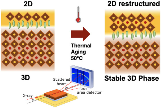
Engineering 2D/3D perovskite interfaces is a common route to realizing efficient and stable perovskite solar cells. Whereas 2D perovskite’s main function in trap passivation has been identified and is confirmed here, little is known about its 2D/3D interface properties under thermal stress, despite being one of the main factors that induces device instability. In this work, we monitor the response of two typical 2D/3D interfaces under a thermal cycle by in situ X-ray scattering. We reveal that upon heating, the 2D crystalline structure undergoes a dynamical transformation into a mixed 2D/3D phase, keeping the 3D bulk underneath intact. The observed 3D bulk degradation into lead iodide is blocked, revealing the paramount role of 2D perovskite in engineering stable device interfaces.
Within the past decade, hybrid perovskites (HPs) have sat at the forefront of the most recent advances in the area of a new generation semiconductors for cheap optoelectronics, skyrocketing the field of photovoltaics with their power conversion efficiency beyond 25%.1 Critical device stability is currently a well-known issue for market uptake.2−8 Behind the most recent advances, engineering multidimensional perovskite interfaces has been revealed as an interesting approach to improving the lifetime of HP devices, mainly due to the improved humidity resistance of the 2D layer.9−19 Examples span from large aminovaleric-acid-based cations,20 to widely used phenylethylammonium,21 butylammonium iodide, octylammonium iodide, and dodecylammonium iodide (DAI) cations,22 to fluorous-based cations23,24 synthesized ad hoc to improve robustness against water and, more recently, to thiophene-based cations.25 In most cases, 2D perovskites simultaneously act as a surface defect passivant layer and retard charge recombination at the interface with a positive effect on device open-circuit voltage.21−30 On top, as previously mentioned, 2D perovskites show high humidity resilience due to their increased chemical stability and hydrophobicity, which slows down device degradation.31−34 However, so far, little is known about the role of 2D perovskite upon thermal stress, which is also a recognized cause of perovskite device degradation. This calls for a deep understanding of the interface behavior upon heating, which is crucial to assess device stability.35 Here we address this need by an in-depth investigation of the 2D/3D film properties during thermal stress, monitoring the structural evolution of the interface and the related optoelectronic and dynamical properties as well as the full device behavior.
We performed combined in situ grazing-incidence wide-angle X-ray scattering (GIWAXS) with steady-state and time-resolved photoluminescence (PL) measurements on two study cases of 2D/3D perovskite systems used in the most common highly efficient device configuration.21,25 They consist of a bulky thiophene- or phenyl-terminated cations in the form of 2-thiophenemethylammonium iodide (2-TMAI) or phenylethylammonium (PEAI), forming (2-TMAI)2PbI4 and PEA2PbI4 2D perovskites, respectively, which overlayer the bulk 3D perovskite. (See Figure 1a.) The structural evolution of the interface is monitored upon exposing the sample to a thermal cycle, simulating the working conditions under real device operation. We reveal that a slow dynamical variation of the 2D/3D interface manifests, leading to a structural modification of the 2D perovskite structure. In concomitance, the 3D perovskite bulk, if protected by the 2D layer, is unperturbed, whereas in the absence of the 2D layers, it shows visible signs of structural degradation. We thus identified a key role of the 2D capping layer in blocking the thermal degradation of the 3D perovskite bulk, maintaining its structural integrity and retarding thermally induced degradation in perovskite solar cells.

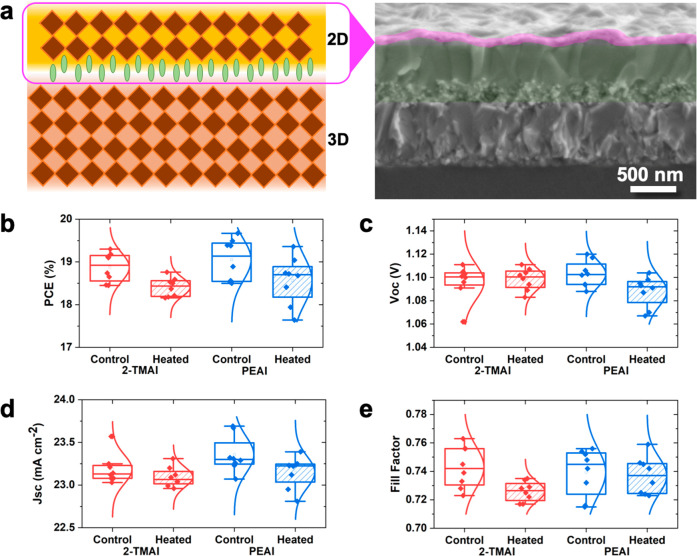
(a) Cartoon of the 3D/2D interface (left) and the corresponding cross-sectional SEM image of the 3D/2-TMAI 2D interface. (b–e) Statistics of the device photovoltaic properties (PCE, Voc, Jsc, FF) by comparing the fresh device and the thermally aged devices heated according to the thermal cycle shown in Figure 2.
To create the 2-TMAI- (or PEAI-) 2D/3D thin films and devices, we dissolved the organic salts in isopropanol (IPA) and dynamically spin-coated them on the top of a triple-cation [(FAPbI3)0.87(MAPbBr3)0.13]0.92(CsPbI3)0.08-based 3D perovskite film, where MA stands for methylammonium and FA stands for formamidinium. (See the Supporting Information for details.) As a result, a thin layer of 2D perovskite (∼60 nm) was formed on top of the 3D bulk, as shown by the scanning electron microscope (SEM) image in Figure 1a (right). Whereas the main focus was the study of the interface structural modification, we also fabricated 2-TMAI-2D/3D and PEAI-2D/3D solar cells, and we tested them upon the same thermal cycle as that used for the in situ measurements. Statistics on device current–voltage characteristics and photovoltaic parameters are reported in Figure 1b–e and Table 1, respectively. It is interesting to note that upon thermal stress, the device characteristic is not dramatically affected, showing no massive effect of the thermal stress on the device efficiency. A small decrease is observed only for the device fill factor, which, however, does not dramatically reduce the overall device performance. Table 1 reports the device parameters comparing the fresh and the “heated” device. This contrasts with common knowledge of 3D perovskite solar cells, showing a demonstrated reduction in device performance upon heating.36 (See Table S1.)

| treatment | Voc (V) | Jsc (mA cm–2) | FF | PCE (%) |
|---|---|---|---|---|
| PEAI/3D | ||||
| control | 1.10 ± 0.01 | 23.4 ± 0.2 | 0.74 ± 0.02 | 19.1 ± 0.5 |
| heated 50 °C, 100 min | 1.09 ± 0.01 | 23.2 ± 0.2 | 0.74 ± 0.01 | 18.6 ± 0.6 |
| 2-TMAI/3D | ||||
| control | 1.10 ± 0.02 | 23.2 ± 0.2 | 0.74 ± 0.02 | 18.9 ± 0.3 |
| heated 50 °C, 100 min. | 1.10 ± 0.01 | 23.1 ± 0.1 | 0.73 ± 0.01 | 18.4 ± 0.2 |
To get deeper insights into the 2D/3D interface role under thermal stress and its structural stability, we carried out in situ GIWAXS (measurements performed at the Brazilian Synchrotron National Laboratory (LNLS) in the XRD2 beamline; see Supporting Information for additional data) during a temperature cycle, as schematically shown in Figure 2a. In particular, the experiment was performed under thermal annealing conditions and an inert atmosphere (N2), adopting the following thermal cycle: First, we raised the temperature to 100 °C after the deposition of the large organic cations and kept it constant for 6 min; then, we decreased it to 50 °C and kept it constant for 160 min. (See the top chart in Figure 2b,c.)
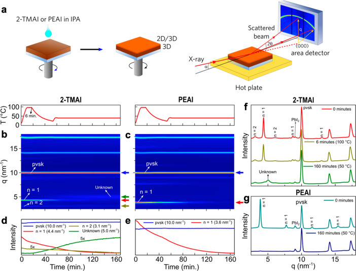
(a) Cartoon drawing illustrating the deposition of 2D perovskite on top of 3D perovskite and the schematic drawing of the in situ GIWAXS measurement. (b,c) In situ GIWAXS diffraction maps as a function of time and temperature for 2-TMAI and PEAI modified perovskite (pvsk) films, respectively. (d,e) Respective intensities of the main peaks as a function of time. (f,g) Respective X-ray diffraction patterns at different times.
Upon the spin coating of the 2D cation on top of the 3D perovskite, just after dropping the solution and in the beginning of the thermal annealing (Figure 2f, 0 min), we clearly observed the immediate appearance of new peaks at low q values of 4.4 and 3.1 nm–1 for 2-TMAI. These features correspond to first-order peaks of 2D perovskite layers.25 They refer to a different structure of the 2D perovskite forming isolated single (n = 1) inorganic layers spaced by the large cation, giving the diffraction at 4.4 nm–1, and to a mixed phase (commonly known in literature as quasi-2D or mixed 2D) where more than one inorganic layer (in this case, it is well-defined with n = 2) is held together and intercalated by the large cation, giving the diffraction at 3.1 nm–1, respectively. For the PEAI-2D-based interface, a single n = 1 2D phase is formed, leading to the formation of a pure PEA2PbI4 2D layer, confirmed by the first-order peak at q = 3.6 nm–1.
In both cases, with thermal aging, the intensity of the n = 1 peak decreases (Figure 2d,e) and vanishes in the time window investigated for 160 min (Figure 2f,g). This reveals a dynamical change of the 2D perovskite layer structure under thermal stress, which loses its n = 1 crystalline phase. In the case of 2-TMAI-2D/3D, the intensity of the n = 2 peak also decreases (Figure 2d,f); however, in this case, a new peak emerges in concomitance with the reduction of 2D peaks. This happens after 20 min, manifested as a new broader peak at a q value of 5.0 nm–1 (Figure 2b, green curve), which keeps increasing during the thermal aging at 50 °C and reaches a plateau. This peak it is not related to a 2D phase, as for the comparison of the pure n = 1 and 2 2-TMAI-based 2D perovskites. (See Figure S1.) Moreover, it is not related to any quasi-2D perovskite with a n > 2 structure, suggesting that a mixed intermediate structure is formed at the interface. The more detailed procedure for calculating the peaks and their calculated values with n > 2 can be found in the Supporting Information and in Table S4, respectively.
On the contrary, in the case of PEAI-2D/3D, no further evolution is observed upon thermal aging. Figure 2 also reports the diffraction signal related to the 3D perovskite structure. It is remarkable to notice that the mutation alters only the 2D superficial layer, whereas the 3D perovskite underneath remains unaltered and stable (Figure 2d,e). Repeating the same measurements for the bulk 3D perovskite, the behavior is strikingly different: In this case (see Figure S2), the 3D peak decreases by 15% in magnitude, revealing a clear material degradation upon heating, in agreement with common knowledge. On the contrary, when the 2D overlayer is present (Figure 2d,e), for 2-TMAI and PEAI, no reduction was observed. This provides compelling evidence of the fundamental role of the 2D perovskite in enhancing the robustness of the 2D/3D system, with a special focus on improving the thermal stability of the 3D perovskite underneath.
To confirm and better elucidate the structural changes in the 2D layer, we monitored the PL spectral evolution as a sensitive probe of the material band gap and the variation thereof, which is indicative of any possible structural change (i.e., n variation), following a similar thermal cycle, as shown in Figure 3.
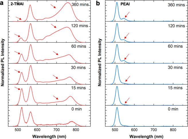
PL spectra of (a) 2-TMAI-2D/3D and (b) PEAI-2D/3D perovskite thin films upon thermal aging at 50 °C and excitation at 450 nm from the front (in other words, from the 2D side).
Because the PL spectra were recorded from the front side (2D perovskite side) of the 2D/3D film, they mainly show the emission from the 2D perovskite top layers. The PL measurements were carried out after thermal annealing at 100 °C and without heating to 50 °C (time 0 for PL characterization). At time 0, the 2-TMAI-2D/3D film PL spectrum shows two emission bands centered at 519 and 567 nm, whereas the PEAI-2D/3D film shows only one band at 510 nm and a small shoulder at 555 nm. According to literature, these bands correspond to the emission from n = 1 and 2 phases of 2D perovskites, respectively,25,37 in excellent agreement with the GIWAXS results. From the normalized PL spectra reported in Figure 3, it is also evident that for the 2-TMAI-2D-based interface a broader emission in the 700–800 nm spectral range gradually appears during the annealing process. This suggests the formation of a mixed disordered phase,38,39 in agreement with the GIWAXS data. On the contrary, for PEAI-2D/3D, the variation of the shape of the PL spectra is less dominant, whereas the absolute intensity (reported in Figure S3a) of the n = 1 PL peak abruptly diminishes, in agreement with the GIWAXS data. This suggests that PEAI-based 2D perovskite is structurally more robust and less prone to forming a quasi-2D (n > 1) phase under this conditions.12,40 A similar behavior of the intensity is observed for the 2-TMAI-2D-based interface, showing a decrease in the n = 1 PL peak and a concomitant increase in the broader emission at the longer wavelength side (Figure S3b). These measurements prove the dynamical variation of the 2D surface perovskite band gap. To gain a deeper understanding of the mechanism behind such dynamical structural/band gap evolution, we also measured the PL spectra of the 2D/3D perovskite films upon aging the film for a long time window of 7 weeks without any heating. The films were stored in a dark and dry environment (RH < 20%) at room temperature, and the PL spectra were periodically recorded over time. Interestingly, we observed an analogous modulation of the emission features for both 2-TMAI-2D/3D and PEAI-2D/3D over slow dark aging, as shown in Figure S4. This phenomenon indicates that a similar transformative process happens even at room temperature, over a several weeks time window, while being accelerated under thermal stress. We can rationalize our results considering an intrinsic dynamical evolution of the 2D/3D perovskite interface upon aging, which manifest as (i) destructuration of the 2D perovskite overlayer and (ii) the formation of an additional mixed phase at the interface, both combined with (iii) improved resilience to the degradation of the 3D perovskite bulk underneath, independent of the 2D cation used.
Finally, it is worth pointing attention to the fact that device performance with the 2D overlayer does not dramatically decrease upon heating, despite the interface structural rearrangement. This is due to the role of the 2D perovskite, which preserves the 3D bulk nature and function. To better analyze the interfacial processes, we implemented time-resolved PL (TrPL), with the idea of monitoring the charge-carrier dynamics in the 3D bulk upon the thermal cycle. The thermal aging for the TrPL measurement was performed under the same condition as in the steady-state PL measurement. The results are reported in Figure 4 for the 2D/3D interface (blue and red) compared with the controller samples without the 2D layer. It is worth noting that upon thermal aging, the PL signal of the bare 3D film shows an enhancement of the lifetime with a marked long living tail. This happens at time 0 but is even more evident after 15 min of annealing, and it continues to increase up to 360 min of thermal aging (Figure S5). This is also true for the 2D/3D interface, where the increase in the lifetime is even more evident. We can attribute the longer living signal to the beneficial effect of the restructuring of the interface, leading to the surface passivation effect and retarded surface charge-carrier recombination.38,41
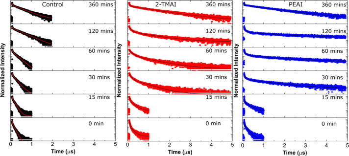
TrPL decays (λexc = 440 nm; F = 9.7 nJ cm–2; λPL at the maximum of the 3D at 780 nm emission at 50 °C in the samples) of the 2D/3D modified perovskites: 3D control (black), 2-TMAI (red), and PEAI (blue). The fits of the decays are also shown.
In conclusion, the in situ structural and optical analysis of 2D/3D perovskite interfaces and devices gives compelling proof of an intrinsic dynamical structural variation of the 2D perovskite layer after thermal stress, which (i) protects the 3D perovskite from degradation regardless of the 2D perovskite phase evolution upon heating, (ii) does not perturb the dynamical processes at the interface, and (iii) is beneficial to keeping the device performance unaltered under thermal stress. Our results have highlighted the key role of the 2D surface functionalization in retarding perovskite degradation upon thermal stress, providing a clear direction on how to gain perovskite device longevity.
Supporting Information Available
The Supporting Information is available free of charge at https://pubs.acs.org/doi/10.1021/acs.nanolett.0c01271.
Materials and methods, calculation of XRD peak position, Tables S1–S4, and Figures S1–S8 (PDF)
Author Contributions
A.A.S. fabricated thin films and PSCs and characterized them. N.D. designed and synthesized the organic salts. R.S., P.E.M., J.C.G., and H.C.N.T. performed the in situ GIWAXS analysis. V.I.E.Q. performed PL measurements. J.C.G. performed TrPL measurements. G.G. and A.F.N. conceived the idea. A.A.S., R.S., G.G., and A.F.N. designed the experiments. A.A.S., R.S., G.G., and A.F.N. wrote the manuscript. G.G., A.F.N., and M.K.N. supervised the project. All authors reviewed the paper.
Notes
The authors declare no competing financial interest.
Acknowledgments
We thank the LNLS for providing beamtime at the beamline XRD2. R.S. thanks the São Paulo Research Foundation (FAPESP, grant 2017/12582-5). R.S., J.C.G., and A.F.N. gratefully acknowledge support from the FAPESP (grant 2017/11986-5) and Shell and the strategic importance of the support given by the ANP (Brazil’s National Oil, Natural Gas and Biofuels Agency) through the R&D levy regulation. A.F.N. also acknowledges CNPq. We acknowledge the Swiss National Science Foundation (SNSF) funding through the Synergia Grant EPISODE (grant no. CRSII5_171000). G.G. acknowledges the “HY-NANO” project that has received funding from the European Research Council (ERC) Starting Grant 2018 under the European Union’s Horizon 2020 research and innovation programme (grant agreement no. 802862).