 Unraveling
the Ultrafast Hot Electron Dynamics in
Semiconductor Nanowires
Unraveling
the Ultrafast Hot Electron Dynamics in
Semiconductor Nanowires
ACS Nano


- Altmetric
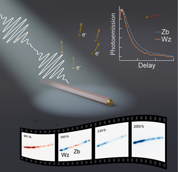
Hot electron relaxation and transport in nanostructures involve a multitude of ultrafast processes whose interplay and relative importance are still not fully understood, but which are relevant for future applications in areas such as photocatalysis and optoelectronics. To unravel these processes, their dynamics in both time and space must be studied with high spatiotemporal resolution in structurally well-defined nanoscale objects. We employ time-resolved photoemission electron microscopy to image the relaxation of photogenerated hot electrons within InAs nanowires on a femtosecond time scale. We observe transport of hot electrons to the nanowire surface within 100 fs caused by surface band bending. We find that electron–hole scattering substantially influences hot electron cooling during the first few picoseconds, while phonon scattering is prominent at longer time scales. The time scale of cooling is found to differ between the well-defined wurtzite and zincblende crystal segments of the nanowires depending on excitation light polarization. The scattering and transport mechanisms identified will play a role in the rational design of nanostructures for hot-electron-based applications.
The properties of photogenerated hot carriers have been studied intensely, the incentive being that utilizing their excess energy could be highly beneficial for a wide range of applications such as hot-carrier-driven catalysis,1−3 light sensing,4,5 and solar energy conversion.6,7 In all these applications, the use of hot carriers competes with their ultrafast relaxation via a variety of scattering mechanisms. The evolution of the hot carrier distribution in space and energy is therefore important for their efficient extraction and usage,8,9 and an understanding of this evolution is crucial for guiding the design of future hot-carrier-based devices. For such devices, the use of nanomaterials is highly favorable as they allow for a strong concentration of hot carriers10,11 and can be engineered to reduce carrier–phonon scattering rates, thus extending hot carrier lifetimes.12,13 This has sparked intense research on ultrafast hot carrier dynamics in various materials, such as plasmonic nanoparticles,14 III–V semiconductor materials,15 and lead-halide perovskites.16,17 III–V semiconductor nanowires (NWs), in particular, allow for the combination of several functional materials into a single nanostructure, enabling the creation of tailored energy filters for hot electron extraction.18,19 This, in combination with the high degree of control over the NW growth process, makes these nanostructures a promising platform for hot-carrier-based semiconductor devices and for exploring the fundamental processes governing carrier transport and relaxation.
A typical hot carrier device uses a nanostructure as light absorber7,20 from which the electrons and/or holes are then extracted. It is worth considering the multitude of processes, whose interplay governs hot carrier relaxation in such a system on different time and length scales. Interaction of an ultrashort light pulse with a semiconductor leads to the coherent excitation of free states in the conduction band, with the transition rates depending on material band structure and properties of the light field.21 Fast (∼fs) dephasing of this initial excitation occurs via carrier–carrier and, to some extent, carrier–phonon scattering, resulting also in momentum randomization of the excited electron distribution.22,23 Initially, the carriers are localized in energy due to the finite spectral width of the excitation light. However, energy redistribution of the excited carriers, primarily via carrier–carrier scattering, rapidly leads to energy broadening and eventually to the formation of a hot thermal distribution,17,24 typically within tens of fs, with a temperature that can be substantially higher than the lattice temperature (thermalization). Subsequently, energy relaxation of the hot carriers leads to cooling of the hot distribution until thermal equilibrium with the lattice is reached. Various scattering mechanisms such as electron–phonon scattering, electron–hole scattering,25,26 or impact ionization27,28 may contribute to electron energy relaxation, with electron–phonon scattering typically being the dominant dissipation channel.29 Additionally, transport due to density gradients or electric fields (from external sources or internal fields, e.g., due to interfaces) may change the spatial distribution of the hot carriers over time. Processes related to interfaces are of particular importance in nanostructures with typically high surface-to-volume ratios, especially as these are the regions where hot carriers can be extracted. The importance, time scales, and interplay of the dynamic processes are not generally known, and often studies focus on a single or a few processes. Electron–phonon interaction, for example, has been identified as important in hot electron devices and is at the focus of a large body of work investigating carrier cooling on the ps time scale.29−32 However, cooling via electron–hole scattering is typically not explicitly examined in recent studies, even though it can constitute a major energy loss channel,25,26 in particular in semiconductor materials with different effective mass for electrons and holes, and has thus important implications for the function of hot carrier devices.
Studies exploring the ultrafast behavior of hot carriers mostly employ transient absorption spectroscopy or other spatially averaging techniques to investigate bulk systems or nanoparticle ensembles. While optical techniques are well-suited for capturing averaged carrier dynamics, their spatial resolution is restricted by the optical diffraction limit, making it challenging to probe nanoscale variations of dynamics within nanostructures and devices. These spatial variations certainly influence the response of nanophotonic systems.33 This can be particular problematic in semiconductor-based hot electron devices which combine several nanoscale components of different materials, for example, hot carrier solar cells.
Recent years have seen the emergence of various ultrafast time-resolved microscopy techniques combining the excellent time resolution of the optical pump–probe approach with high-resolution imaging beyond the diffraction limit, such as scattering-type scanning near-field optical microscopy34,35 or ultrafast electron microscopy.36 Among these techniques is time-resolved photoemission electron microscopy (Tr-PEEM),37 where high-resolution images are formed by photoelectrons emitted from the sample. In Tr-PEEM, excitation and probing of the sample are timed by ultrashort laser pulses, making the technique an ideal candidate for pushing the time resolution of ultrafast microscopy to the few-fs38,39 regime and beyond.40 Early studies using Tr-PEEM have focused on investigating plasmonic near fields in metallic nanoparticles and nanostructured films.41−43 More recently, the technique has also been applied to the study of charge carrier dynamics at semiconductor surfaces and interfaces.44−49
Here, we implement Tr-PEEM to visualize hot electron transport and cooling in single InAs NW heterostructures with a time resolution of 30 fs. We observe signatures of rapid hot electron transport toward the NW surface driven by an internal electric field and estimate how this process effects the evolution of hot electron distribution in the nanowires. We go on to find that the excess energy of the hot electron distribution is dissipated via electron–hole and electron–phonon scattering. In particular, the importance of electron–hole scattering has not been considered in a number of previous studies. Finally, we demonstrate variations in the hot electron relaxation between NW segments of the same material, but different crystal phase, depending on the polarization of the excitation light. The detailed spatiotemporal study allows us to evaluate the processes underlying the hot electron dynamics in this system, identifying which processes are dominant and how fast they occur. This enables insights into hot electron dynamics in complex nanostructures and should be valuable for the design of future hot electron devices.
Results and Discussion
We investigate the relaxation dynamics of photoexcited hot electrons in InAs NWs with an axial stacking of wurtzite (Wz) and zincblende (Zb) segments. Detailed investigations of the NW atomic scale structure, morphology, and electrical properties have been carried out previously.50 Briefly, the NWs with a diameter of 100 nm consist of a center Zb segment with {110}-type facets between two Wz segments above and below featuring mainly {1010} and {1120} side facets, respectively (as sketched in Figure 1a), with a low number of stacking faults in all segments. The NWs are inherently n-doped due to carbon incorporation during the growth process.51 Downward surface band bending leads to the formation of an electron accumulation layer at the NW surface with an estimated carrier concentration of ∼2 × 1018 cm–3 (see Methods section). A scanning electron microscopy (SEM) image of a typical NW is presented in Figure 1b, showing the axial stacking of Wz and Zb segments and the gold seed particle atop the NW.

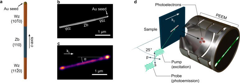
InAs NW sample and Tr-PEEM setup. (a) 3D sketch of the InAs NW showing the axial stacking of Wz and Zb segments. The predominant crystal facets are indicated for each of the NW segments. (b) Scanning electron microscopy (SEM) image of an InAs NW with axially stacked segments of Wz and Zb crystal structure. The NWs used in this study have a length of 2.85 μm and a diameter of 100 nm. (c) Tr-PEEM image of the NW shown in (b) acquired with a time delay of Δt = 100 fs between pump and probe pulses. k∥ is the propagation direction of the incident light projected onto the sample plane, as shown in panel (d). The angle between the NW axis and k∥ is α ≈ 13.5°. The bright spots visible at the ends of the NW are due to field enhancement around the gold seed particle atop the NW and at a sharp edge at the NW base. (d) Schematic of the Tr-PEEM setup. A pump pulse (2.27 eV) excites the sample. A probe pulse (2.27 eV) arriving at a variable time delay after the pump induces photoemission of hot electrons. These are then imaged in PEEM, creating a high-resolution image of the NW. Arrows indicate the different polarizations used (s- and p-polarization).
The experimental scheme for hot electron imaging using Tr-PEEM is illustrated in Figure 1d. We optically excited single InAs NWs using 24 fs pump pulses centered at 2.27 eV (545 nm), creating a nonequilibrium distribution of photoexcited electrons. The photon energy of 2.27 eV considerably exceeds the material bandgap of 0.35 eV for Zb InAs at room temperature.52 The bandgap of Wz InAs is slightly higher,53 and a previous study determined a difference of 36 meV between the Zb and Wz segments of the NWs investigated here.50 The excitation results in an initial electron distribution with an excess energy of ∼1.60 eV with respect to the conduction band minimum, as determined from ab initio calculations of the photoexcitation rate in Wz and Zb InAs (details are given in Section S1 of the SI). The photoexcited holes only obtain a small fraction of the excess energy (∼0.4 eV) due to their higher effective mass as compared to the conduction band electrons.54,55 To observe the hot electron dynamics, we use a second 24 fs probe pulse (2.27 eV), arriving at the sample at a variable time delay Δt after initial optical excitation (see Figure 1d). Hot electrons that reside above a threshold energy ET (∼1.4 eV above the conduction band minimum, see Methods section) can be photoemitted by the probe pulse in a one-photon process and are subsequently imaged with down to 50 nm spatial resolution by the PEEM, as shown in Figure 1c.
Thus, we create images that directly reflect the evolution of the high-energy tail of the hot electron distribution in the conduction band. A schematic depiction of the pump–probe process is given in Figure 2. The probe region is also limited in real space due to the finite inelastic mean free path of the excited electrons. For a pump/probe photon energy of 2.27 eV, we estimate an inelastic mean free path of 4 nm; that is, the experiment is sensitive to hot electron dynamics in the vicinity of the NW surface (see Methods section). Further, we note that the in-plane component of the electron momentum (with regard to the surface the electrons are emitted from) is also conserved during the photoemission process. The relatively small probe photon energy implies that photoemission is allowed only for electrons with k-vectors nearly perpendicular to the NW surface, corresponding to the direction for the Zb segment and the () direction for the upper (lower) Wz segment, respectively. This selectivity is illustrated in more detail in Figure 2c, which shows the probed energy–momentum region for the Zb segment. By design, the experiment thus selectively probes the evolution of the hot electron distribution in a well-defined energy, momentum, and spatial region. This results in very low levels of background signal and enables us to focus on the dynamics of the energetic hot electrons near the surface region, which are highly important for the efficiency of hot electron devices. More details on the experiment can be found in the Methods section.
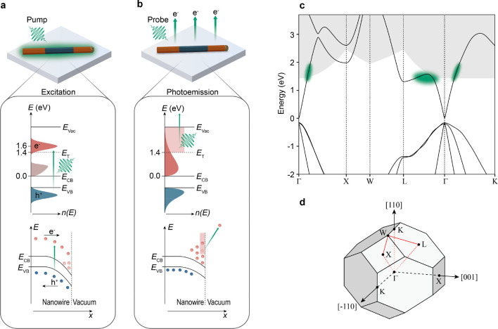
Schematic depiction of the interaction between NWs and the pump and probe pulse. (a) Optical excitation of the NW. The distribution of the photoexcited carriers in energy (top) and space (bottom) is illustrated. The electrons are initially excited at ∼1.60 eV above the conduction band minimum and distributed throughout the entire NW. A cold background distribution of electrons is present in the conduction band due to the intrinsic n-doping of the NW (light red), forming an electron accumulation layer at the NW surface. (b) After excitation, the electrons undergo thermalization and cooling, as well as transport to the NW surface due to an internal electric field. The probe pulse can only induce photoemission of electrons within the high-energy tail of the electron distribution (above the threshold energy ET, shaded red) and within the surface region of the NW (red shading, bottom panel). The photoemitted electrons are imaged in the PEEM. (c) Band structure of Zb InAs. The green highlights indicate areas in the conduction band where electrons are initially excited (see SI section S1). The shaded area indicates the energy-momentum region from which electrons can be emitted by the probe pulse in a one-photon process (probe window). The region has been evaluated for the Brillouin zone path shown in (d) considering momentum and energy conservation in the photoemission process. (d) Brillouin zone of Zb InAs. For the evaluation of the probe window, emission from the (110) surface was considered.
To follow the relaxation of the hot electrons in time, we record a series of PEEM images as a function of pump–probe delay as shown in Figure 3a. Here, both optical pulses have the same linear polarization (p-polarized, as indicated in Figure 1d). In order to emphasize changes in the photoelectron intensity, a reference image recorded at a time delay of 50 fs has been subtracted. Only images acquired at time delays Δt ≥ 50 fs are included in the analysis to ensure that pulse overlap effects are negligible. At Δt = 50 fs, in the instant after photoexcitation, a large photoemission yield is observed due to photoexcited hot electrons with large excess energy populating the conduction band after excitation by the pump pulse. From 50 to 150 fs a further increase of the photoemission yield from the NW is observed until the maximum intensity is reached (Figure 3a and b). The rapid initial rise is followed by a slower decay of the hot electron signal during the remaining measurement range of ∼6 ps. Even though the polarization configuration used here (pump and probe p-polarized) results in very similar dynamics in the Wz and Zb segments of the InAs NW, small variations between the segments of different crystal structure can be found, as discussed further below.
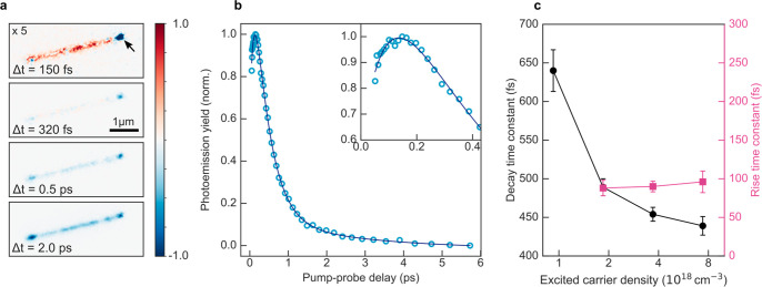
Hot electron dynamics in a single InAs nanowire. (a) Time-resolved PEEM images taken at different pump–probe delay times. The images show accumulation (red) and depletion (blue) of hot electrons with respect to the reference image taken at a time delay of 50 fs (not shown). The arrow marks the position of the gold seed particle. Further images are shown in the SI (Section S2). (b) Time evolution of the photoemission yield averaged over the entire InAs nanowire (not including the gold particle) and multiexponential fit (solid line). (c) Time constant of the fast decay component and the rise component as a function of excited carrier density.
For more detailed quantitative analysis, the photoemission intensity is averaged over the NW and plotted as a function of pump–probe delay as shown in Figure 3b for a pump fluence of 5.3 μJ/cm2, corresponding to an excited carrier density of 1.9 × 1018 cm–3, or 4 × 10⁴ excited electrons per NW as estimated from finite difference time domain calculations (see Methods section). The evolution of the photoemission intensity can be decomposed into three stages: (i) an initial rise followed by (ii) a dominant fast decay and (iii) a slower decay component of smaller amplitude (by a factor of ∼10) than the fast decay. From multiexponential fitting we obtain a rise time of 120 ± 10 fs and decay time constants of 400 ± 10 fs and 2.7 ± 1.4 ps for the fast and slow decay, respectively. To further elucidate the physical origin of the individual components, we investigate the excitation density dependence of the dynamics. As shown in Figure 3c, we find that the time constant of the dominant decay component decreases with increasing excited carrier density, from 640 ± 40 fs at n = 0.9 × 1018 cm–3 to 440 ± 30 fs at n = 7.4 × 1018 cm–3. The time constant of the initial rise component is practically constant within the investigated fluence range. The relative amplitude of the rise, however, becomes smaller with decreasing excited carrier density, with the rise not being observable for an excitation density of n = 0.9 × 1018 cm–3 (see SI, Section S3).
Electron energy-resolved photoemission measurements provide further insight into the evolution of the hot electron distribution. We employ a variable high-pass filter such that only photoelectrons with kinetic energy exceeding the filter cutoff contribute to the Tr-PEEM images. Energy-filtered Tr-PEEM measurements of a single InAs NW are presented in Figure 4. At low cutoff values (Figure 4a), the dynamics resemble the energy-integrated measurements featuring a rapid initial rise (90 ± 20 fs) followed by a pronounced decay (430 ± 30 fs). The slow decay component could not be evaluated due to a reduced measurement range. At higher cutoffs (Figure 4b), the photoemission intensity decays more rapidly (260 ± 20 fs), revealing an increase of the hot electron relaxation rate with energy. In addition, we find that the ∼100 fs rise is absent when monitoring the high-energy tail of the electron distribution, showing that the rise signal is due to the electrons in the lower part of the probed energy window (between ET and ET + 0.7 eV), while no further accumulation of hot electrons occurs at higher energies (above ET + 0.7 eV).
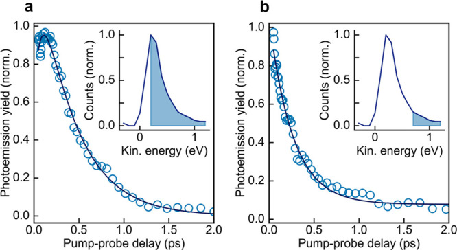
Energy-resolved Tr-PEEM measurements of hot electron dynamics. Photoemission yield as a function of pump–probe delay with kinetic energy cutoff at 0.2 eV (a) and 0.7 eV (b). Experimental data are shown as open circles, whereas solid lines represent (multi-)exponential fits. In both panels, the inset shows the energy distribution of the photoelectrons emitted at a pump–probe delay of 50 fs. The shaded area indicates the portion of the electron distribution above the cutoff energy.
The evolution of the photoemission intensity from the NW (Figure 3b) is a direct consequence of the dynamics of the high-energy part of the hot electron distribution within the surface region of the NW, with the dynamic components reflecting different stages of the hot electron relaxation. We now discuss the initial rise of the photoemission intensity, which reveals accumulation of hot electrons in the probe window within the first ∼150 fs after photoexcitation.
First, we consider if electron–electron scattering can provide a plausible explanation for this observation. The initial energy distribution of the optically excited electrons, determined by the material band structure and the energy profile of the exciting pulse, is nonthermal; that is, it is not possible to assign an electron temperature at this point. However, the distribution rapidly evolves into a thermal, Fermi–Dirac distribution via electron–electron scattering (thermalization), a process that is associated with a redistribution of the conduction band electrons over a wide energy range.17,24 This process could conceivably provide a mechanism for the observed rise, supposing that during thermalization electrons scatter into initially unoccupied (or only partly occupied) states above the detection threshold (ET) of the Tr-PEEM experiment. This requires that the initial photoexcited electron distribution be centered below the detection threshold in energy (E0 < ET). While simple modeling based on the Boltzmann equation, describing electron thermalization and cooling within the relaxation time approximation, can reproduce the energy-integrated Tr-PEEM measurements (see Section S4 of the SI), several experimental observations challenge the assignment of the rise component to thermalization via electron–electron scattering. First, the requirement that E0 < ET for the rise to appear is in contradiction to the relative placement of E0 and ET established above and in the Methods section (E0 ≈ 1.6 eV and ET ≈ 1.4 eV with respect to the conduction band minimum). Second, the thermalization rate is expected to become faster at larger photoexcited carrier densities, which disagrees with the observed lack of density dependence of the rise time (Figure 2c). Finally, if the rise was caused by a gradual population of high energy states due to thermalization, the rise should be visible at all photoelectron energies (as discussed further in Section S4 of the SI). This, however, is in direct contrast to the energy-resolved Tr-PEEM measurements (Figure 3), which show that the rise is absent at high cutoff energies.
We thus conclude that electron thermalization is most likely not at the origin of the fast electron accumulation. Electron–electron scattering must occur, but we suggest that the electrons can already be described by a thermal distribution for the time delays considered here (Δt ≥ 50 fs). We estimate that the initial temperature of the hot electron distribution is ∼2600 K for an excited carrier density of 2 × 1018 cm–3 (see Section S5 of the SI). The fast thermalization time is consistent with recent work on hot carrier transport in InAs NWs, which extracts electron–electron scattering times on the order of ∼10 fs,18 and with time-resolved studies on GaAs substrates, which reported thermalization faster than 100 fs56 or even within tens of fs24,57 for carrier densities similar to those created in our experiments.
To explain the observed early time behavior, we need to consider the NW surface and its effect on the hot electron distribution. InAs surfaces are well-known to exhibit Fermi level pinning above the conduction band minimum.58 For intrinsically n-doped InAs NWs with a native oxide layer, the conduction band minimum was shown to be positioned at ∼0.2 eV below the Fermi level at the NW surface,59 resulting in downward band bending and the formation of an electron accumulation layer at the NW surface. The band bending is associated with an internal electric field, which, after optical excitation, drives transport of the photoexcited electrons (holes) toward the surface (interior) of the NW until the electric field is (partly) screened,60 as illustrated in Figure 2a and b. This results in band flattening, which persists until the photoexcited carriers have recombined. Clear evidence of band flattening can be seen in Tr-PEEM images taken at later time delays where the hot electron signals have completely decayed (10 ps and later), thus providing evidence for the accumulation of photoexcited electrons in the NW surface region (for details see Section S6 of the SI). On the basis of the above considerations and taking into account the high surface sensitivity of PEEM (see Methods section), we propose that the rise in photoemission yield reflects this accumulation of electrons near the NW surface due to field-induced hot electron transport. The ∼100 fs time scale of the rise component agrees well with experimental and theoretical studies on GaAs,60,61 which reported field-induced ultrafast electron transport to the surface on similar time scales for comparable excitation densities. The lack of electron accumulation at high cutoff energies (Figure 3b) then implies that the most energetic electrons lose a portion of their energy during transport, leading to a rise component only at lower cutoff energies. This agrees with the work by Dekorsy etal., which explained field-induced transport in GaAs in terms of a drift-diffusion model,60 suggesting that electron drift—rather than ballistic motion—is the mechanism underlying the ultrafast hot electron transport; that is, the electrons scatter several times before reaching the NW surface. This is consistent with an electron–electron scattering time in InAs nanowires of ∼10 fs, as determined by Chen etal.,18 which is significantly shorter than the observed rise time, implying that several electron–electron scattering events may occur during transport.
Finally, we comment on the absence of the rise component at the lowest excitation density and the density-independent rise time constant in the context of field-induced hot electron transport. Calculations of charge–density profiles inside GaxIn1-xAs NWs (x = 0.05) show that the electrons become more confined toward the surface as the excitation density increases.59 At lower excitation densities, on the other hand, the accumulation layer is less pronounced and extends further into the NW. This effect, in combination with the surface sensitivity of Tr-PEEM, can explain the disappearance of the rise component at low excitation density since the transport dynamics are unfolding further away from the NW surface in this case. In addition, the electron concentration in the accumulation layer varies nonlinearly with excitation density,59 possibly leading to variations in the relative rise amplitude with excitation density. Further, the disappearance of the rise could indicate that the electrons arriving at the surface are below the energy range accessible by the probe pulse. The initial thermalization of the photoexcited electrons with a cold background distribution (due to n-doping of the NW) leads to a lower initial temperature of the hot electron distribution at lower excitation densities. This, in turn, results in a lower fraction of electrons above the detection threshold energy, making it more likely that these electrons lose energy in scattering events during transport to the surface region. Previous studies on bulk GaAs60 have shown that electron transport in surface fields occurs faster at higher excitation densities. However, the dependence is highly nonlinear and becomes more flat for excitation densities comparable to those used here,60 possibly explaining why no clear density dependence of the rise time was observed in our measurements. In addition, the nanoscale dimension of the NW in the radial direction (which is relevant here) might alter the transport dynamics as compared to bulk systems. Detailed theoretical investigations considering Fermi-level pinning, the microscopic properties of Wz and Zb InAs and their effects on hot electron transport, and the nanoscale dimensions of the system would provide further insight into the details of the transport and screening dynamics beyond the scope of the present work.
Now we turn our attention to the next steps of the dynamics. The thermalized hot electron distribution undergoes energy relaxation via different scattering mechanisms such as electron–phonon scattering, defect scattering, impact ionization, or electron–hole scattering, eventually leading to thermal equilibration of the hot electron distribution with the lattice. This cooling process is directly reflected by the decay in photoemission yield from the NW (Figure 3b), since a decrease in electron temperature Te is associated with depletion of hot electrons above the detection threshold of the experiment and, thus, a lower number of photoelectrons ejected by the probe pulse. The energy-resolved Tr-PEEM measurements reveal an increased relaxation rate at higher cutoff energy, as expected for hot electron cooling.29 However, the time constants of the decay must be interpreted with care since only the high-energy tail of the hot electron distribution contributes to the signal. This implies that the measured signal decays at a higher rate than the average electron temperature. On the basis of model calculations that assume exponential decay of the electron temperature, described in detail in the SI (Section S5), we estimate a factor of ∼0.2 between the decay time of photoemission yield and the decay time of the electron temperature; that is, the decay time constants τ1 = 400 ± 10 fs and τ2 = 2.7 ± 1.4 ps characterizing the decay of the photoemission yield from the NW (Figure 3b) correspond to a decay of the electron temperature on time scales τ′1 ≈ 2 ps and τ′2 ≈ 14 ps.
To understand the cooling process, we need to consider various scattering mechanisms that may contribute to energy relaxation of the hot electrons and identify the dominant contribution based on the experimental evidence. For the fast cooling, electron–phonon scattering must be considered since it is typically an important dissipation mechanism for hot electron cooling and can lead to relaxation times of only few hundreds of fs,62 especially at high electron excess energies,15 as in the present case. However, pump–probe measurements at different pump fluences show that the dominant decay is faster at higher excitation densities (Figure 3c). This carrier density dependence suggests that the fast temperature decay cannot be attributed to only electron–phonon scattering, for which the scattering rate should be density independent or even decrease with density in case the excitation fluence is sufficiently high for hot phonon effects to occur.29 Likewise, we can conclude that impact ionization, which can be relevant for energy relaxation in narrow-bandgap materials such as InAs28 or InSb,27 is not the main relaxation mechanism since it is also density independent.63 Scattering by defects can be excluded as well, since most of these scattering events are elastic. Instead, the density dependence indicates that the fast cooling is strongly influenced by carrier–carrier scattering. As already established, electron–electron scattering likely occurs on a much shorter time scale for any plausible hot electron density, and we must therefore consider electron–hole scattering. Due to the large difference in effective mass between electrons and holes in InAs, the electrons obtain most of the excess energy after above-bandgap excitation. The electron temperature Te will thus exceed the hole temperature Th after internal thermalization within each subsystem (electrons and holes), so that inelastic collisions between electrons and holes will effectively lead to a cooling of the hot electron distribution.25,26,64 Generally, electron–hole scattering is expected to occur on a few-ps time scale,29 in agreement with the fast temperature decay time. The mechanism also provides an explanation for the observed two-stage cooling behavior as the rate of electron cooling decreases once electrons and holes are in equilibrium (Te ≈ Th), as shown in previous studies on p-doped GaAs.26,65 While we observe a clear increase in decay rate at higher densities, we note that the dependence is not as pronounced as expected from theoretical considerations,66,67 which predict a decay time inversely proportional the excited carrier density. A less pronounced dependence on carrier density has been found for GaAs22,23 and can be attributed to screening of the Coulomb interaction. A more detailed quantitative understanding of the carrier-density-dependent behavior would require further theoretical work carefully considering the interactions including impact ionization and phonon scattering effects. In conclusion, the data indicate that there is a strong contribution from electron–hole scattering to the fast cooling based on the carrier density dependence and the presence of two time constants in the hot electron decay curve. This is corroborated by previous work that predicted that the energy loss rate from electron–hole scattering can exceed electron–phonon losses for carrier densities above ∼1018 cm–3 in GaAs.25 Further discussion of electron–phonon scattering and impact ionization can be found in Section S7 of the SI. The significant difference between the time scales cooling via electron–hole scattering for thermalization via electron–electron scattering (<50 fs) can be rationalized by the large difference in effective mass between electrons and holes in InAs and the spatial separation of the photoexcited electrons and holes driven by the internal electric field. Most III–V semiconductors have very significant differences between electron and hole masses, so that electron–hole scattering should occur broadly in these materials at high excitation densities. Finally, we remark that we rule out contributions from intervalley scattering processes because scattering from the Γ-valley to the L-valley is presumably too fast to be registered at delays Δt ≥ 50 fs and electrons scattering back to the Γ-valley are below the detection threshold of the experiment, as discussed further in the SI (Section S8).
On longer time scales, further cooling of the hot carriers takes place until thermal equilibrium with the lattice is reached. The ∼14 ps time scale of the slow cooling roughly agrees with the time scales found in previous studies on hot phonon dynamics in bulk InAs,68,69 and we thus assign this component to hot electron cooling via phonon emission. Finally, we note that Yang etal.70 have shown that surface trap states situated roughly at 0.5 eV above the conduction band minimum lead to hot electron trapping in InAs nanowires. This mechanism can also cause depletion of hot electrons in the probe window and could thus result in a decay of the photoemission yield with increasing pump–probe delay. Thus, while it is plausible to assign the slow decay component to cooling via electron–phonon scattering, we cannot fully exclude contributions from electron trapping. The pump fluence dependence of the fast decay component, on the other hand, clearly points toward carrier–carrier scattering and excludes electron trapping as its cause.
In summary, we arrive at the following picture of hot electron relaxation in InAs NWs within the first few picoseconds after excitation: (i) Thermalization of the initial photoexcited electron distribution via electron–electron takes place within tens of fs, leading to the formation of a hot Fermi–Dirac distribution of electrons in the conduction band. (ii) On a time scale of ∼100 fs, hot electron transport from the inside of the NW toward the surface occurs, driven by the internal electric field which is a result of the Fermi-level pinning at the NW surface. The transport is not ballistic, but accompanied by electron–electron scattering, such that electrons in the high-energy tail of the distribution lose a portion of their energy. (iii) Subsequently, the hot electron distribution cools down mostly via electron–hole scattering, with an estimated temperature decay time of about 2 ps. (iv) On longer time scales, further cooling of the hot electrons takes place (temperature decays on a ∼14 ps time scale), likely due to electron–phonon scattering.
Having established the general interpretation of the Tr-PEEM signals in InAs NWs, we now consider the dependence of the hot electron dynamics on the nanowire crystal phase and excitation pulse polarization. Results from Tr-PEEM measurements with horizontally polarized (p-polarized) excitation pulses are shown in Figure 3. The NW is oriented at an angle of 13.5° with respect to the plane of incidence, as indicated in Figure 1, so that horizontal (p) polarization results in an electric field component in the direction parallel to the NW axis with an amplitude E∥ ≈ 0.4E0 where E0 is the total field amplitude. Vertically (s) polarized light, by contrast, is oriented perpendicular to the NW axis such that E∥ ≈ 0. Tr-PEEM images recorded at different delay times after excitation with horizontally polarized pulses (Figure 3a) show that the evolution of the photoemission intensity is roughly homogeneous along the NW without pronounced differences between the Wz and Zb segments. The photoemission yield from the NW segments reaches it peak value at the same time delay after photoexcitation and exhibits very similar decay dynamics (see Figure 5a). Excitation with s-polarized light, by contrast, results in a significant spatial variation of the hot electron dynamics, as shown in Figure 5. A comparison of the kinetic traces from the Zb segment and the bottom Wz segment of the NW (Figure 5b) shows that s-polarized excitation leads to distinctly slower hot electron relaxation in the Zb segment as compared to Wz. These variations are also directly visible in Tr-PEEM images, as shown in the SI. To characterize the spatial variation in hot electron dynamics in more detail, we extract the time constant of the fast photoemission intensity decay as a function of position along the NW axis, as shown in Figure 5c and d. The results reveal a direct correlation between hot electron dynamics and crystal phase.
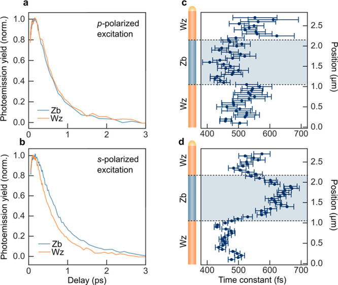
Polarization dependence of hot electron dynamics. (a, b) Kinetic traces showing the evolution of the photoemission yield from the Zb and lower Wz segment for p-polarized (a) and s-polarized (b) excitation. The probe pulse is p-polarized in both cases. Traces are normalized to peak value. (c, d) Time constant of the (fast) decay component as a function of position along the nanowire for p-polarized (c) and s-polarized (d) excitation.
The average decay time constants for the three segments of the NW for different excitation conditions are summarized in Table 1. For p-polarized excitation, the photoemission yield from the Zb segment decays more rapidly as compared to the top/bottom Wz segment, while the opposite is the case for s-polarized excitation. In addition, a comparison of the two Wz segments shows that the decay dynamics are slightly faster in the bottom segment, independent of pump polarization.

| pump polarization | pump fluence | τWz,top | τWz,bottom | τZb |
|---|---|---|---|---|
| p-pol. | 5.3 μJ/cm2 | 560 ± 20 fs | 520 ± 20 fs | 470 ± 10 fs |
| s-pol. | 10.6 μJ/cm2 | 530 ± 10 fs | 460 ± 10 fs | 630 ± 10 fs |
Evidently, the polarization of the pump pulse affects the time scale of the dominant (fast) decay of the photoemission intensity, which we have attributed to depletion of electrons in the probe window due to electron cooling mainlyvia electron–hole scattering. This scattering mechanism is associated with a density-dependent cooling rate, which, in turn, suggests that the polarization-induced variations in the decay dynamics can be attributed to differences in the photoexcited carrier density. The polarization dependence of the NW’s optical response is governed by two mechanisms. First, the elongated shape of NW causes attenuation of electric fields perpendicular to NW,71,72 leading to a generally lower photoexcitation density for s-polarized excitation in our experimental geometry. Second, the microscopic anisotropy of the Wz lattice gives rise to a polarization dependence of dielectric function (and thus excitation probabilities) at certain optical frequencies,73,74 while Zb InAs has nearly isotropic optical properties75 due to its cubic crystal structure. The difference in relaxation rate in the Zb segment between s- and p-polarized excitation thus reflects the first mechanism, i.e., attenuation of the electric field due to the NW shape. Variations within the NW, on the other hand, can be attributed to the anisotropic optical properties of Wz InAs. This is in agreement with calculations of the Wz InAs dielectric function (see SI, Section S9), as well as previous theoretical work by De etal.,76 both predicting stronger absorption at 2.27 eV for light polarized perpendicular to the Wz c-axis, as discussed in detail in the SI (Section S9). Finally, we consider the difference in relaxation rate between the top and bottom Wz segments of the NW. The two Wz segments of the NWs have different surface facet terminations. Previous studies using secondary electron X-ray PEEM50 have shown small variations in work function between the top and bottom Wz segment of the NWs. In the Tr-PEEM experiments discussed here, this would affect the position of the threshold level ET and thus give rise to small differences in the observed dynamics (see SI, Section S5), which provides an explanation for the observed differences between top and bottom Wz segments.
Conclusions
We have employed Tr-PEEM to image the ultrafast hot electron dynamics within single, structurally well-defined InAs NWs. We identified signatures of inelastic hot electron transport to the NW surface region within ∼100 fs after excitation and characterized the electron cooling process. We observed two stages of the cooling, fast and slow, which we attribute to mainly electron–hole and electron–phonon scattering, respectively. Using the spatial resolution of the Tr-PEEM, we find small but distinct variations in the hot electron relaxation dynamics between NW segments of Zb and Wz crystal phase depending on the excitation light polarization. These differences are explained in terms of the anisotropic optical properties of Wz InAs, leading to polarization-dependent differences in absorption rate between Zb and Wz segments.
The redistribution in energy and space of the hot electrons as observed in the present study should be considered in the design of devices that exploit hot carriers. Given that surface-induced band bending is a common feature of semiconductors, the carrier transport toward the surface within ∼100 fs and the resulting hot carrier accumulation will influence optimum design of contacts for hot carrier extraction. The energy relaxation of the hot electrons via electron–hole scattering indicates that this scattering mechanism is a significant energy dissipation channel for hot electron cooling in InAs NWs and potentially in other materials with a large effective mass ratio between electrons and holes. Energy transfer between hot electrons and holes has a significant influence on the function of hot carrier solar cells77 and should therefore be taken into consideration in the design and construction of such devices. For example, a recently much investigated approach to improving the efficiency of hot electron devices relies on slowing down hot electron cooling via phonon emission by increasing the excitation density78 (hot phonon bottleneck effect79). At the same time, however, higher excitation densities may lead to an increased rate of energy transfer from electrons to holes via electron–hole scattering, thus effectively cooling the hot electrons, which might offset favorable effects from reduced electron–phonon scattering. Fast hot electron cooling via electron–hole scattering might also impede the efficient population of conduction band side valleys, which has been suggested as an alternative route to achieve extended hot carrier lifetimes.8,9
Lastly, hot carrier devices combine several components such as light absorbers, energy filters, and contacts on the nanoscale, and the ability to spatially map the femtosecond hot electron dynamics provides intriguing possibilities for the characterization of such devices.
Methods
Tr-PEEM Measurements
For imaging with high spatiotemporal resolution, we combined a commercial PEEM (IS-PEEM, Focus GmbH, lateral resolution down to ∼40 nm) with an optical pump–probe approach. Pump and probe pulses at 2.27 eV (545 nm) with a full width at half-maximum (fwhm) of 0.1 eV (25 nm) were generated in a noncollinear parametric amplifier (NOPA) seeded by a Yb:KGW amplified laser system (Pharos, Light Conversion) delivering 170 fs pulses at 1030 nm with 30 μJ pulse energy at up to 200 kHz repetition rate. Pulses generated by the NOPA had a pulse duration of 24 fs (fwhm), as determined from intensity autocorrelation measurements. For the time-resolved measurements, the NOPA output was split into two replicas with controllable time delay between the pulses. The polarization of pump and probe pulses was controlled independently by variable waveplates in the beam path. The beams were focused onto the sample under an angle of incidence of 65° (with respect to surface normal), which results in an elongated spot size of approximately 90 μm × 45 μm, leading to homogeneous excitation conditions across the entire NW. To reduce the background of multiphoton photoemission, pump and probe pulse energies were reduced to typically ∼0.5 nJ per pulse using neutral density filters. Tr-PEEM images were recorded with typical exposure times of ∼5 min per image, at a pressure of around 1 · 10–9 mbar and with an image resolution in the range from 50 to 200 nm. Tr-PEEM measurements are surface sensitive since the short electron inelastic mean free path (typically a few nm for electrons with E < 10 eV in inorganic materials80) limits the escape depth of the excited electrons. After interaction with pump and probe pulse and prior to photoemission, the electrons have an energy of ∼4 eV with respect to the conduction band minimum, with a corresponding mean free path of approximately 4 nm in InAs.80 Another important parameter of the Tr-PEEM measurements is the threshold energy ET since if defines which portion of the electron distribution can be photoemitted by the probe pulse. Based on the work of Chellappan etal.81 on native oxide-covered InAs (100) surfaces, we assume an electron affinity of ∼3.7 eV, which places the threshold ET at (3.7 eV – 2.27 eV) ≈ 1.4 eV above the conduction band minimum (CBM); that is, the initial population of photoexcited electrons (at ∼1.6 eV above CBM, as determined from ab initio calculations of the photoexcitation rate at 2.27 eV photon energy) is situated above the detection threshold ET in energy. The electron affinity of InAs varies between surface facets50 and depends on surface oxidation,81 and thus a precise placement of the detection threshold ET is challenging. However, we observe a two-photon photoemission process at hν = 2.27 eV, which is consistent with the initial electron population being situated above ET.
Sample Fabrication
Our sample consisted of InAs NWs with an axial stacking of wurtzite and zincblende segments. The NWs were grown on InAs substrates using metalorganic vapor phase epitaxy, and sharp switching between Wz and Zb segments was achieved by controlling the group V precursor flow, as described by Lehmann etal.82 Further details regarding NW growth and a detailed description of the NW morphology and electrical properties can be found elsewhere.50 The NWs are covered by a thin native oxide layer and are intrinsically n-doped due to carbon incorporation during NW growth. A donor density of n ≈ 2 × 1017 cm–3 was estimated from scanning tunneling spectroscopy measurements on unreconstructed and defect-free NW surfaces by Hjort etal.50 for NWs from the same growth batch. The presence of a native oxide layer on the NWs investigated here leads to Fermi-level pinning and the formation of an electron accumulation layer at the NW surface.83 For the given donor density, calculations of the charge density profile in the NW83 suggest a carrier concentration of n ≈ 2 × 1018 cm–3 in the electron accumulation layer. For the Tr-PEEM experiments, the NWs were transferred onto (weakly) n-doped silicon substrates for imaging. The same individual NWs investigated in Tr-PEEM experiments were afterward imaged in a scanning electron microscope to inspect the NW morphology.
Finite Difference Time Domain Simulations
To estimate the number of photoexcited electrons per pulse and NW, we numerically determined the NW absorption cross section σNW using classical electrodynamics simulations based on the finite difference time domain (FDTD) method. Calculations were performed using the FDTD Solutions software from Lumerical. We employed a total field scattered field plane wave source with broadband spectrum and enclosed the simulation volume with perfectly matched layers. The NW was assumed to be homogeneous (no segment structure), and the dielectric function of InAs was taken from the literature.84 For an NW with hexagonal cross section and a length of 2.85 μm placed on a glass substrate we obtained the cross sections σNW∥ = 0.28 μm2 and σNW⊥ = 0.18 μm2 at 545 nm (2.27 eV) for light polarized along and perpendicular to the NW axis, respectively. For a typical pump fluence of 5 μJ/cm2, this results in a photoexcited carrier density of 1.9 × 1018 cm3, or approximately 4 × 10⁴ electron–hole pairs per NW (polarization along the NW axis).
Electronic Structure Calculations
To determine band structure, density of states, photoexcitation rates, and dielectric function of Wz/Zb InAs, we performed DFT calculations with the ABINIT electronic structure code85,86 and corrected the band structure by self-consistent quasi-particle GW calculations. To obtain a finer sampling of the band structure in k-space, we constructed the Wannier functions of the system using the Wannier90 package.87 The density of states was obtained through Wannier interpolation.
Supporting Information Available
The Supporting Information is available free of charge at https://pubs.acs.org/doi/10.1021/acsnano.0c08101.
Initial distribution of photoexcited electrons (S1); Tr-PEEM images at various time delays (S2); Tr-PEEM measurement at different excitation fluences (S3); model for electron thermalization and cooling (S4); estimation of hot electron cooling times (S5); evidence for electron accumulation at NW surface (S6); influence of impact ionization and electron–phonon scattering on fast cooling (S7); intervalley scattering (S8); polarization dependence of cooling dynamics (S9); fluence dependence of photoemission yield (S10) (PDF)
Author Present Address
# E.V.B.: Max Planck Institute for the Structure and Dynamics of Matter, Luruper Chaussee 149, 22761 Hamburg, Germany.
Notes
The authors declare no competing financial interest.
Acknowledgments
The authors acknowledge financial support from NanoLund, the Swedish Research Council, the Crafoord Foundation, and the Knut and Alice Wallenberg Foundation.