Nature Communications

- Altmetric
There is an emergent demand for high-flexibility, high-sensitivity and low-power strain gauges capable of sensing small deformations and vibrations in extreme conditions. Enhancing the gauge factor remains one of the greatest challenges for strain sensors. This is typically limited to below 300 and set when the sensor is fabricated. We report a strategy to tune and enhance the gauge factor of strain sensors based on Van der Waals materials by tuning the carrier mobility and concentration through an interplay of piezoelectric and photoelectric effects. For a SnS2 sensor we report a gauge factor up to 3933, and the ability to tune it over a large range, from 23 to 3933. Results from SnS2, GaSe, GeSe, monolayer WSe2, and monolayer MoSe2 sensors suggest that this is a universal phenomenon for Van der Waals semiconductors. We also provide proof of concept demonstrations by detecting vibrations caused by sound and capturing body movements.
The Gauge factor (GF) enhancement in strain sensors remains a key challenge. Here the authors leverage the piezoelectric and photoelectric effects in a class of van der Waals materials to tune the GF, and obtain a record GF up to 3933 for a SnS2-based strain sensor.
Introduction
Electronic strain gauge sensors were invented by E. E. Simmons and A. C. Ruge in 1938 to measure the strain and deformation experienced by objects. Recently, due to the rapid development of soft robots, remote monitoring, artificial intelligence, and wearable health care devices, there has been surge in demand for high-flexibility, high-sensitivity, and low-power strain gauges that can monitor and sense small deformations and vibrations in extreme conditions1–16. The sensitivity metric of a strain gauge, known as the gauge factor (GF), is defined as:

In this work, we report a strategy to tune and enhance the GF of strain sensors based on VdWLMs by controlling the carrier density and mobility via photo excitation. A gauge factor of as high as 3933 is found for a SnS2 based strain sensor, which is five times higher than the GF value reported for strain sensors based on VdWLMs and exceeds the GF value reported for ZnSnO3 nanowires4,9. Moreover, the GF can also be tuned over a wide range of values, between 23 and 3933. Our observations indicate that it is a universal phenomenon for Van der Waals semiconductor materials, demonstrated by measurements on a representative group of materials including SnS2, GaSe, GeSe, monolayer WSe2, and monolayer MoSe2. We also provide two real world demonstrations for our sensors, by using a prototype to detect tiny vibrations caused by sound and the normal daily movement of a human body.
Results
Giant gauge factor of SnS2 based strain sensors
Figure 1a shows a schematic of a Van der Waals strain sensor device. To prepare the devices, the VdWLMs are transferred onto polydimethylsiloxane (PDMS) substrates. Details of the device fabrication can be found in the Supplementary Information. The characterization of the strain devices was performed utilizing a commercial strain-testing platform in atmosphere at room temperature. The strain was applied by elongating or bending the PDMS substrates. Since the PDMS substrate and Van der Waals material sensor are bonded together with the metal electrodes, the strain experienced by the sensors will be approximately equal to that applied to the PDMS substrate33,36–38. In order to inject nonequilibrium carriers, a 365 nm light was used to excite electron-hole pairs in the VdWLMs. Supplementary Fig. 1 shows an optical image of a SnS2-based strain sensor. The thickness D of the crystalline SnS2 flake is around 60 nm and the distance between electrodes is around 30 µm. Figure 1b plots the characterization of I–V behavior of the SnS2-based strain sensor under various strain conditions measured in darkness. The I–V curves are asymmetric and show distinct nonlinear behavior, indicating a Schottky barrier is formed between SnS2 and metal electrodes. Moreover, the I–V curves shift downward with applied tensile strain, suggesting strain can modify the electrical transport properties of the sensor. It is worth noting that the Schottky contacted devices are reported to have much greater responsivity than Ohmic contacted devices.39–41 To evaluate the device performance,

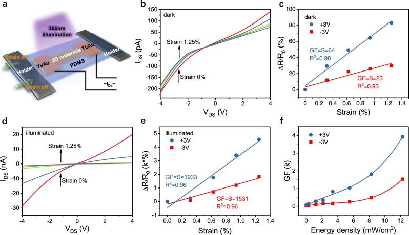
Giant gauge factor (GF) of SnS2 based strain sensors.
a Schematic of the Van der Waals strain sensor devices. b
I–V curves under various strain conditions measured in darkness. c The variation of
Origin of enhanced GF value by photo illumination
The downward shift of the nonlinear I–V curves in Fig. 1b and d clearly indicate that the carrier transport through the SnS2/metal interfaces and SnS2 channel region is affected by the strain as well as by the photo illumination. The device band profile is illustrated in Supplementary Fig. 2 and considering the electrons flowing from the left-hand side to the right-hand side, the reverse-biased diode at the first contact (1) dominates the device current. There are three transport mechanisms for majority carriers to cross a metal-semiconductor contact junction: (i) diffusion of carriers from the semiconductor into the metal, (ii) thermionic emission of carriers across the Schottky barrier, and (iii) quantum-mechanical tunneling through the barrier42–44. For a low-doped semiconductor or at high temperature the tunneling current is comparatively negligible45. In these situations, the transport of majority carriers in sensor device mainly results from diffusion and thermionic emission, and the current through the device can be described by classical thermionic emission-diffusion theory8,9:


L is the channel length, p (n) and μp (μn) are the hole (electron) density and mobility, respectively, and we simply assume
Since S, A**, T, ND, and Vbi are insensitive to strain deformation, the variation of current with strain (s) is mainly a result of changes in the SBH and channel resistance (CR) due to the piezoelectric effect. At high bias, the equivalent potential variation (EPV, the exponent part of Eq. (2)) caused by the changes of SBH and CR is given by:


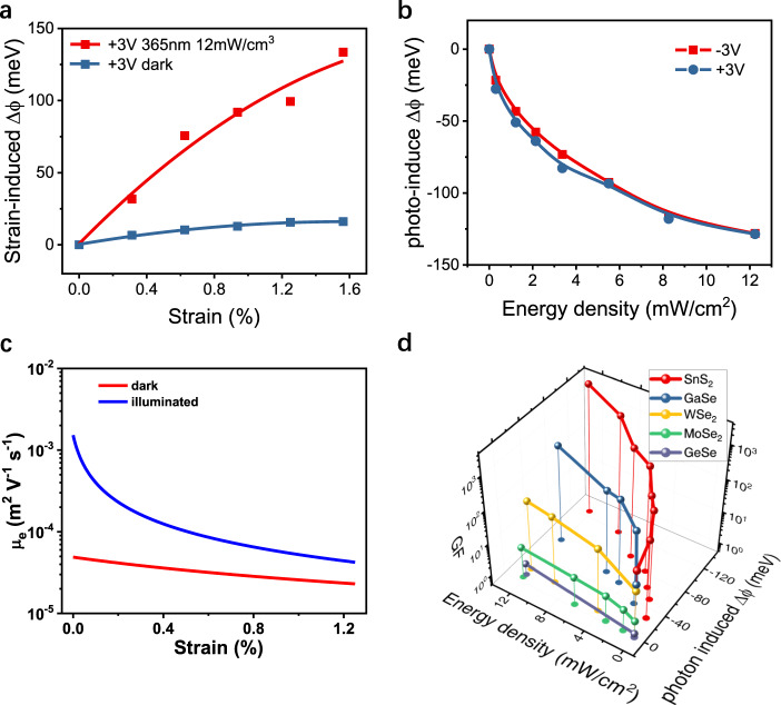
Origin of enhanced GF value by photo illumination.
a Calculated relative change of equivalent potential variation (
Figure 2b shows that the EPV at zero strain decreases with increasing the laser power density. In addition, the current responses of a SnS2 based strain sensor in a continuous extruding and stretching test, as shown in Supplementary Fig. 4, indicates that the resistance of the sensor does increase greatly with stretching strain but decreases with extruding. The best fit of EPV for these currents, in proportion to s1/2, is linear in darkness but parabolic under illumination. This indicates that the strain current in darkness is mainly dominated by CR because the SBH depends linearly on the strain (discussed later).
In order to analyze these phenomena, let us first study the strain distribution within the SnS2/PDMS system, and calculate the electronic and optical properties of SnS2 under such strain. The stress and strain distributions are calculated by using a stationary solid-mechanics model performed in COMSOL Multiphysics tools (for details, see Supplementary Information). Supplementary Fig. 5a plots the simulation structure. The distribution of the von Mises stress (Supplementary Fig. 5b) for an applied stretching force shows that the SnS2 nanosheet encounters a larger stress than the PDMS due to the much higher Young’s modulus (56 gigapascals) of SnS2 compared to PDMS (0.75 megapascals), resulting in upwards bending displacement. However, the downwards bending displacement under an extruding force is not significant (Supplementary Fig. 5c). The principal-strain vector distribution on the SnS2 surface (Supplementary Fig. 5d) and the strain distributions (Supplementary Figs. 6 and 7) for the directions along and normal to the natural plane for a cross-sectional line, show that there is a shear strain normal to the natural plane. This stress-induced structural bending for a system with two contrasting hardness materials is schematically shown in Supplementary Fig. 6.
Based on these results, we calculated the band structure, dipole moment, absorption coefficient and refractive index for the unstressed structure and the normal- and shear-stressed structure using density functional theory (DFT) performed in the CASTEP code (details, see Supplementary Information). For a strain s < 1%, the bandgap variation (Supplementary Fig. 8 and Supplementary Table 1) is only tens of milli electron volts (meV), much smaller than the bandgap (2.2 eV) of SnS2, and therefore would not significantly change SnS2 resistance and its SBH. In addition, for a strain s < 1%, variations of absorption coefficient, and refractive index (Supplementary Fig. 9) are ~4.6% and ~0.2%, respectively, which would also not appreciably change the photoelectric effect in SnS2. Consequently, best candidate mechanism responsible for photo-induced giant gauge factor is the piezo-phototronic effect.
The dipole moment of a SnS2 nanosheet under normal and shear stresses was calculated using Mulliken charge, as shown in Supplementary Table 1, which indicates that there is a nonzero dipole moment distributed not only in the force direction but also in the c axis (z-direction) for the bending SnS2 nanosheet. The dipole (piezo) charge in the force direction appears on the sidewalls of the nanosheet, which would be ineffective at increasing the electric current in a top-gated configuration. While the c-axis piezo-charge is distributed over the top and bottom of the nanosheet creating a piezoelectric field


Notably, (i) the piezo charge is separated by a distance of dipole length Ddp (0.295 nm), while the external charge is separated by the sheet thickness D. (ii) The reversed surface piezocharge under an extruding force offsets the external interface charge resulting in an increased mobility μ and current.
Based on Matthiessen’s rule, the total mobility can be calculated by the equation

μ0 (
Apart from the modification of the carrier mobility, the carrier density injected by the photoelectric effect also modifies the equivalent doping density ND in Eq. (2), that is

The currents with respect to strain for dark and 365 nm laser illumination conditions are calculated by inserting Eqs. (3), (10), and (11) into Eq. (2) and then solving self-consistently. The calculated results are summarized in Fig. 3. Although the calculated results show some differences when compared with the experiment values, the theoretical model still demonstrates that the key mechanism in sensitivity enhancement is the screening effect of photocarrier on piezoelectric field, suppressing the boundary scattering. The overestimation of the strain effect (Fig. 3) in this simple classical model may be refined by considering the quantum interference effect, especially, in thinner region as shown in Supplementary Fig. 11a (the sensitivity as a function of SnS2 thickness). Supplementary Fig. 11a also shows that the thickness of the layered material dominates the degree of the screening effect and the sensitivity enhancement as observed in our measurements of the thinner WSe2 and MoSe2 samples (Supplementary Figs. 13 and 14), even with the different material parameters. It is worth noting that the observable nonzero current under the zero bias and zero strain in darkness may originate from the displacement current (Idisp) in swept-measured mode56, according to equation

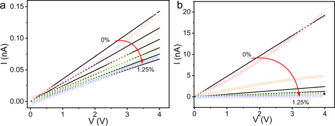
Model of measured sensor currents.
Calculated currents (black lines) and measured currents (colored symbols) for a selection of strains for a dark and b 365 nm laser illuminating conditions.
Our experiments further indicate the enhancement of the GF by photo illumination is a general phenomenon for Van der Waals semiconductor materials. Figure 2d summarizes the GF values of strain sensors based on a variety of Van der Waals semiconductor materials as a function of light power density, for materials including SnS2, monolayer WSe2, monolayer MoSe2, GaSe, and GeSe devices (Supplementary Figs. 13–16). The GF value of a GaSe based sensor is enhanced from 24 to 400. However, for monolayer WSe2 and monolayer MoSe2, the GF enhancement is less than 5. A possible explanation could be an increase of short-range interfacial scattering reducing the carrier mobilities in the monolayer devices. For GeSe, the I–V curves are quite linear for a variety of strain conditions, indicating a small Schottky barrier height between the electrodes and GeSe, as shown in Supplementary Fig. 15d. Note, the Gauge factors measured in dark are 64, 24, 15.2, and 1.7 for SnS2, GaSe, monolayer WSe2 and monolayer MoSe2, respectively. Those values are in the same range as those reported in the literature since the GF values reported for various types of van der Waals strain sensors are normally limited to well below 3003,6,7,19,26–28,32,35. We further summarized the change of Schottky barrier and GF for all of the above listed materials (Supplementary Fig. 17). It also suggests that the alteration of the SBH and CR by the piezo-photonic effect plays an important role in the enhancement of the GF value by photo illumination.
Demonstration of real world applications of VdWLM strain sensors
To demonstrate the real world practical ability of our VdWLM based strain sensors, SnS2 based strain sensors were used to monitor tiny vibrations caused by sound and to capture a range of human motion, including facial, wrist, standing-sitting, and walking movements. Benefiting from giant GF values induced by illumination, the strain sensors are able to detect tiny vibrations. The inset of Fig. 4a shows a SnS2 based sensor on PDMS fixed on a rigid frame and the frame assembled above a sound box. Tiny vibrations were generated by playing short tones at different frequencies and were registered by the strain sensor. The sensor produces a strong and clear response under 365 nm light illumination due to the photon enhanced GF phenomenon, contrasting behavior is particularly evident when a comparison is made with the response of the same device under dark conditions, which show only a weak signal. For the response at 64 Hz, the change in relative resistance with illumination reaches ~1700%, a response ~21 times larger than that observed in darkness. To further demonstrate the application of VdWLMs based strain sensors for real world purposes, SnS2 based sensors on PET (polyethylene terephthalate) were also used to monitor different body movements as shown in Fig. 4b. In Fig. 4c, the movement of facial muscles is displayed for six repeated smiles, for a sensor attached to the cheek. For Fig. 4d the sensor monitors the signal generated by bending of a wrist through different positions. In Fig. 4e and f, the sensor is attached to a knee to monitor different ranges of motion. The movement of standing and sitting, is precisely tracked for three cycles, and slow and normal walking paces can be clearly distinguished by their periodic resistance behaviors.

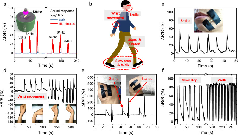
Demonstration of real world application of VdWLM strain sensor.
a The performance of a SnS2 based strain sensor working under illumination when detecting vibrations induced by sound in comparison to signal when working in darkness. b Schematic of strain points produced by motion of a human body used for strain detection by SnS2 based devices. c The measured response produced by smile motion for sensor mounted on cheek, as shown in insert. d Response to wrist bending following positions shown below. e Sensor response to motion of standing and sitting corresponding to the insert image for sensor fixed on knee. f Signals from sensor on knee showing comparative response for slow and rapid walking.
To demonstrate application potential of the strain sensors under repeated and varying strain conditions, we studied the dynamic response of the SnS2 based strain sensors under stretching strain. Similar to the static case, the sensor exhibits a higher strain response under illumination than in darkness. Figure 5a–c show the dynamic response of the SnS2 based device measured under illuminated conditions and an applied cyclic stretching strain (0–0.55% and of frequencies of 0.11, 0.21, and 0.28 Hz). This cyclic movement of strain is achieved by setting the strain-testing platform working at a certain cycling speed. In the second row of Fig. 5a–c displays the associated current trace for each case following their dynamic strain state. In Fig. 5d–f, corresponding Fourier transforms of each of I vs t plots reveal the frequency distribution of the registered strain data. The highest peak indicates their primary oscillation frequency, the other peaks represent higher order natural harmonics and noise within the system.

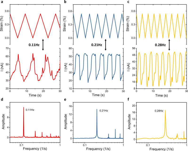
Dynamic strain sensing of SnS2 based strain sensors working under illumination.
a–c The top row shows dynamic strain applied to a sensor at three different frequencies: a 0.11 Hz, b 0.21 Hz and c 0.28 Hz. The second row shows the current response corresponding to each dynamic strain state. d–f The bottom row shows frequencies calculated by Fourier transforms of I–t curve in figure (a–c).
Discussion
We have presented an interesting and apparently universal strategy to tune and enhance the GF of strain sensors based on Van der Waals materials. The GF values can be tuned over a very large range, over 2 orders of magnitude, and a gauge factor value as high as 3933 is achieved for a SnS2 based strain sensor, which has the potential to be further enhanced by increasing light power density. Two types of real world applications, i.e., detecting tiny vibrations caused by sound and daily movements of the human body, were also demonstrated.
Methods
Device fabrication
The SnS2 nanoflakes were transferred by polydimethylsiloxane (PDMS) stamps from a fully covered Si substrate, produced by chemical vapor deposition (CVD)58, to a PDMS bar (Supplementary Fig. 18c). The GaSe and GeSe nanoflakes were mechanically exfoliated from bulk crystals, provide by HQ graphene, and then transferred to a PDMS bar. The monolayer WSe2 was easily removed from Si substrate by immersion in deionized water and floated onto PDMS (Supplementary Fig. 18a)59. The monolayer MoSe2 was transferred by wet transfer60, including: spin coating a polymethyl methacrylate (PMMA) layer onto the SiO2/Si growth substrate for MoSe2, separation of the PMMA/MoSe2 and substrate by a KOH etchant solution, floating MoSe2 crystal onto a PDMS bar and removing the PMMA layer with acetone (Supplementary Fig. 18b). A 30 μm diameter aluminum wire was placed above the target crystal as a shadow mask58. The ends of the wire were fixed with adhesive tape or silver paint. Under a <9 × 10⁻⁶ Pa vacuum condition, 10 nm thick Ti and 140 nm thick Au film were deposited by thermal evaporation. Finally, the adhesive tape and wire were removed.
Numerical calculations
The piezoelectric field combined with the laterally applied field forces the conduction electrons and holes to move in a semicircular or semi-elliptical trajectory due to boundary scattering (Supplementary Fig. 10). Solving the equations of motion in consideration of defect- and phonon-limited relaxations yields an average velocity

The carrier density in VdWLM as a function of local potential is


Thus, we get the Poisson equation


According to the relationship

Solving Eq. (18) and using its result to calculate the mobility, one yields Eqs. (8) and (9). The calculated screened potential and screened electric field in the nanosheet are plotted in Supplementary Fig. 19.
Supplementary information
The online version contains supplementary material available at 10.1038/s41467-021-22316-8.
Acknowledgements
This work was supported by the National Key Research and Development Program under grant Nos. 2017YFA0303800 and 2017YFE0301404, the National Natural Science Foundation of China (No. 61874010), the Science and Technology Innovation Program for Creative Talents in Beijing Institute of Technology (No. 2017CX01006), and by the Ministry of Science and Technology under grant Nos. MOST 108-2628-E-002 -010 -MY3 and 109-2622-8-002 -003.
Author contributions
H.C.W. designed the experiment. W.J.Y. carried out the strain measurements. Y.H.L. and J.C.L. grew the monolayer WSe2 and monolayer MoSe2, respectively. K.M.H. and K.Q.C. performed DFT calculation. T.Y.T and Y.R.W. analyzed the photoelectrical effect. T.H.S. and K.M.H. performed the analysis of the interplay of piezoelectric and photoelectric effects. H.R.F. and C.R.C. gave theoretical advice. D.Z. conducted sample characterization. C.Ó C., S.K.A., Z.W., and Z.T.J. gave experimental advice. H.C.W. wrote the article. All authors discussed the results and commented on the manuscript.
Data availability
The data that support the findings of this study are available from the corresponding author upon request.
Competing interests
The authors declare no competing interests.
References
1.
2.
3.
4.
5.
6.
7.
8.
9.
10.
11.
12.
13.
14.
15.
16.
17.
18.
19.
20.
21.
22.
23.
24.
25.
26.
27.
28.
29.
30.
31.
32.
33.
34.
35.
36.
37.
38.
39.
40.
41.
42.
43.
44.
45.
46.
47.
48.
49.
50.
51.
52.
53.
54.
55.
56.
57.
58.
59.
60.
 Giant gauge factor of Van der Waals material based strain sensors
