
The valley degree of freedom in many-valley semiconductors provides a new paradigm for storing and processing information in valleytronic and quantum-computing applications. Achieving practical devices requires all-electric control of long-lived valley-polarized states, without the use of strong external magnetic fields. Because of the extreme strength of the carbon–carbon bond, diamond possesses exceptionally stable valley states that provide a useful platform for valleytronic devices. Using ultrapure single-crystalline diamond, we demonstrate electrostatic control of valley currents in a dual-gate field-effect transistor, where the electrons are generated with a short ultraviolet pulse. The charge current and the valley current measured at the receiving electrodes are controlled separately by varying the gate voltages. We propose a model to interpret experimental data, based on drift-diffusion equations coupled through rate terms, with the rates computed by microscopic Monte Carlo simulations. As an application, we demonstrate valley-current charge-state modulation of nitrogen-vacancy centers.
In many semiconductor materials, conduction band electrons occupy states near several discrete energy minima (“valleys”). Electrons in these discrete valley states have different properties. For example, the transport properties in applied electric or magnetic fields are dependent on the state. The fact that these states of valley polarization (or valley pseudospin) take discrete values makes the valley pseudospin degree of freedom an attractive resource for all-solid-state quantum information processing (QIP);1 this is a subject that has been termed “valleytronics”,2 in analogy with spintronics for spin-based technology. The topic of valleytronics has attracted considerable attention lately, because of its fundamental interest to the physics community. Creation and detection of valley-polarized electrons have been achieved in several materials, such as in AlAs, where valley polarization was induced by a symmetry-breaking strain,1 in MoS2 by means of polarized light3−6 and in bulk bismuth by using a rotating magnetic field to modulate the population of different valleys.7
The valley polarization in most semiconductors is rapidly destroyed because of the interaction with thermal lattice vibrations. For applications, it is necessary to look for materials where the valley pseudospin relaxation time is exceptionally long. Diamond is a material with a particularly long relaxation time, which is a fact that can be traced back to the extreme hardness of the material, which makes the valley pseudospin robust against lattice deformation and low-energy phonon scattering.8 Previously, it has been demonstrated that valley-polarized states can be created in diamond.9 This occurs by the hot electron repopulation effect in a high electric field or by separating an initially unpolarized population into differently polarized electron states by means of crossed electric and magnetic fields (i.e., via the Hall effect).
However, to realize practical valleytronic applications, establishing a fast, scalable, and direct electrical control of valley states is crucial.10 So far, electrical control of valley transport has not been studied experimentally outside the field of topological transport in low-dimensional materials. In ref (6), Li et al. have demonstrated electrostatic control of valley-polarized currents in a two-dimensional (2D) MoS2 device. In this article, we demonstrate electrical control of valley transport in 3D dual-gate diamond field-effect transistors (FET), where a short UV pulse is used to generate the valley-polarized electrons. We find that it is possible to control the charge current and valley current separately at the receiving electrodes, thereby enabling rapid and scalable valley-current control. We also demonstrate charge-state modulation of nitrogen-vacancy (NV) centers in diamond through valley currents. NV centers in diamond have important applications in, e.g., single-spin magnetometry11 and single-photon sources.12 Our transistors show that it is possible to manipulate the charge states of NV centers locally in devices, just by applying a gate bias voltage.
As mentioned previously, diamond is unique among solids as the extreme rigidity of the lattice leads to highly stable valley states, but diamond also exhibits many other valuable properties for solid-state QIP, e.g., a high electron mobility13 and the existence of the NV center with ultralong spin coherence time.14 The conduction band structure of diamond is similar to that of silicon, with six equivalent conduction band minima oriented along the {100} axes in momentum space. The minima are symmetrically situated at 76% of the distance from the Γ-point to the X-point, as indicated in the energy diagram in Figure 1a. Scattering of electrons between the valleys requires interaction with longitudinal-acoustic (LA) or transverse-optical (TO) phonon modes close to the K-point at the Brillouin zone (BZ) boundary. Because of the rigid covalent bonds in diamond, the K-point LA or TO phonon energies are exceptionally high (∼120 meV). Consequently, the average time between scattering events τf is much longer than in any other semiconductor (∼300 ns at 78 K).8 This is why electrons exist in six different relatively stable valley pseudospin states. On the other hand, because of the lack of an energy barrier, the average acoustic intravalley scattering (scattering within the same valley) time τac is many orders of magnitude shorter (∼1 ps at 78 K).9 Electrons confined to a specific valley have a large ratio between longitudinal effective mass (m||) and transversal effective mass (m⊥), i.e., m|| ≈ 5.5 m⊥.15 This anisotropy makes it possible to separate electrons with different valley pseudospins by their drift in a suitably arranged electric field, as illustrated in Figure 1a. In an applied field (E̅), electrons in separate valleys acquire different drift velocities (v̅). Since intervalley scattering rates are small, this results in a separation of the electron populations.

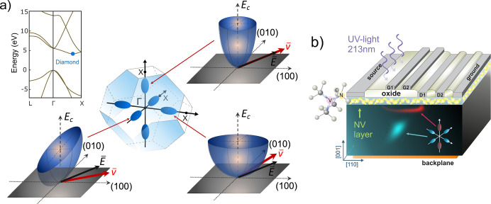
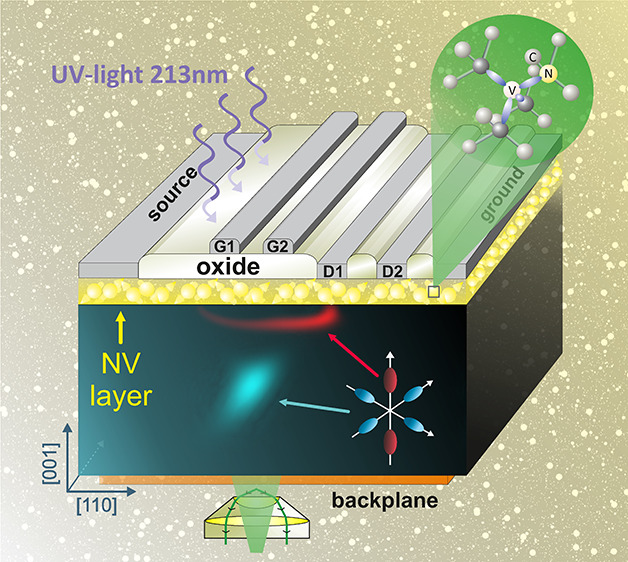
(a) Depiction of the conduction band structure of diamond. The central image of the left figure depicts the first Brillouin zone, together with iso-energy surfaces surrounding the six conduction band minima (“valleys”). The blue dot in the band structure plot (upper left) indicates the position of one conduction band minimum. The remaining images illustrate the energy dispersion of the valleys. Because of the anisotropic effective mass tensors, electrons in different valleys drift in different directions when an electric field is applied. (b) Schematic of a dual-gate two-drain transistor, together with a simulation showing the electron density in different valleys 15 ns after electron injection. G1 and G2 are two independently controllable gates and D1 and D2 are two drains. A thin layer with NV centers is incorporated at the top surface, making it possible to directly image the current density at the contacts through NV center electroluminescence.
To demonstrate electrostatic control of valley pseudospin states, we fabricated field-effect transistors (FETs) using selected single-crystalline diamond plates. These plates were synthesized by Element Six, Ltd., with ultralow nitrogen impurity concentration (<0.05 ppb). FETs in diamond have been studied profusely in recent years,16 but so far they have not been employed to study valley-polarized currents. The designed transistor is depicted in Figure 1b and consists of a source electrode, two gate electrodes isolated from the diamond by a 30 nm Al2O3 dielectric layer, and two drain electrodes at which induced currents can be monitored. The dielectric layer serves both as an insulating gate oxide and as a surface passivation layer, reducing the surface scattering rate and the interface trap density. The dual-gate configuration allows for more control of the valley currents than a single-gate configuration does. The reason for the multiple drain electrodes is that we wish to show that valley-polarized currents can be directed to different locations in the device. With the chosen geometry, drain currents are only induced when charges are drifting in close proximity to the contacts. In contrast to refs (17−20), we emphasize that the electrostatic potential at the gate acts directly through coulomb interaction and is not used to modulate the energy gap or affect the Berry phase. Details of the device processing are described in section S2 in the Supporting Information.
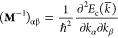
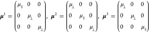
The charge transport was modeled using drift-diffusion and Poisson equations with several electron concentrations, one for each valley in the BZ. Since valleys on the same axis in the BZ have the same effective mass tensor (to quadratic order), the contribution from these valley pairs can be added for simplicity, resulting in three different electron concentrations nl (with valley indexes of l = 1, 2, 3). For low electric fields, the average carrier drift velocity for electrons in the lth valley (v̅l) is proportional to the electric field E̅, i.e., v̅l = μlE̅. Here, the mobility tensor μl for the lth valley pairs is related to the effective mass tensor Ml by μl = q⟨τ⟩(Ml)−1, where q is the elementary charge and ⟨τ⟩ is the average intravalley relaxation time. Since μl is a tensor, the velocity v̅l and the electric field E̅ are generally not parallel. In addition, since v̅l is dependent on the valley index, electrons with different valley pseudospins have a tendency to drift in different directions. The effective mass tensor Ml is given by the curvature of the conduction band, Ec(k̅), at the respective band minima:
An example of a drift-diffusion simulation of the transistor depicted in Figure 1b is shown in Figure 2. Charge is injected at the edge of the source contacts, and states of different valley pseudospin can be seen to drift to different drain contacts. The temperature used for the simulation is 78 K. The simulation shows, for a specific set of bias voltages, the entire process from generation of the charge, to drift and finally detection of the electrons. For this choice of bias voltages, electrons in (001) valleys predominantly drift to D1 while electrons in other valleys are collected at D2. To further investigate this, we recorded the simulated current at drains D1 and D2 for a situation where the voltage at G1 was varied in steps of 0.2 V, and all other bias voltages were held fixed. Note that the current reaches two well-separated peaks at two different times. The contribution to the current from different valley pseudospins is indicated in Figures 3a and 3b by red and blue contours. In this case, the electrons in the (001) valleys travel faster and arrive at the drain contacts earlier than the electrons in the (010) and (100) valleys, resulting in the two peaks.
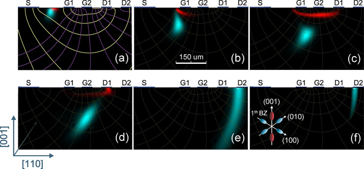
Simulation of valley pseudospin transport in a dual-gate transistor. The simulations shown in panels (a)–(f) show the electron density in different valleys (the red color represents the (001) valleys, and the (010) and the (100) valleys are represented by cyan) at different times (2.5, 8, 13.5, 19, 41.5, and 52 ns, respectively) after optical charge injection at 78 K. The parameters of the applied bias are Vsource = −7 V, VG1 = −5 V, VG2 = −2.4 V, Vbackplane = −2.4 V, with the drains grounded. In panel (a), the inhomogeneous electric field distribution is indicated by purple equipotential lines and yellow field lines.
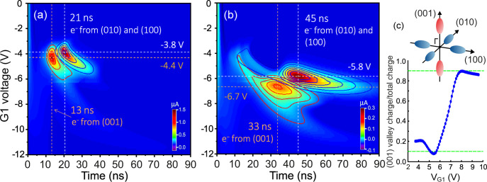
Contour plot of a set of simulated time-resolved total induced currents at (a) D1 and (b) D2. The voltage at G1 is varied between 0 and 12 V, in steps of 0.2 V, and the other bias voltages are fixed: Vsource = −7 V, VG2 = −2.4 V, Vbackplane = −2.4 V, and the drains are grounded. The superimposed red and blue contours specify the contribution to the total current from different valleys. (c) The simulated (001) valley contribution to the total charge collected at drain D2, for the same bias voltages and temperature (78 K) as for panels (a) and (b).
With a suitable choice of gate voltage VG1, it is possible to direct electrons in the (010) and (100) valleys to one contact and (001) electrons to another. Figure 3c shows a simulation of how the degree of valley pseudospin arriving at the second drain (D2) can be modulated by varying the gate voltage VG1. This demonstrates that the contribution of the (001) valleys to the total charge can be modulated with very high fidelity, from 10% to 90% in our devices.
For the experiments, we use a diamond FET with the same geometry and contact configuration as in the simulations. The aim is to compare the drift times obtained in the simulations with the experiments. The diamond transistor was mounted in a cryostat with optical access and kept at a temperature of 78 K. The edge of the source contact was illuminated using a passively Q-switched 213 nm wavelength laser with short pulses (800 ps) and a repetition rate of 300 Hz. In this way, electron–hole pairs were created near the edge of the source electrode by photons with above-bandgap energy (hv = 5.82 eV > Egap = 5.47 eV). To reduce electron–electron scattering to negligible levels, the laser pulse energy was limited to <1 nJ/pulse by an attenuator, resulting in a peak carrier concentration of <1010 cm–3. Below this concentration, the electric field is influenced by the space charge in the electron clouds by <5%. The low power (<0.3 μW) ensures negligible sample heating. The optical excitation creates electron–hole pairs, with the electrons equally populating the six valleys. By applying different negative bias voltages at the source contact, the gate contacts, and the back contacts, the electrons drift toward the drain contacts with different velocities and directions, depending on their valley polarization. The holes are rapidly extracted at the source electrode and their contribution to the drain current is negligible. The induced currents were measured at the drain contacts, which were held at (virtual) ground potential. The induced currents correspond to electron motion in the electric field, in accordance with the Shockley–Ramo theorem.21−23 Further experimental details are given in section S3 in the Supporting Information.
Figure 4 shows measured time-resolved currents from the transistor where we have applied the same set of bias voltages as in the simulation described earlier. The currents originating from longitudinal and transversal valleys are observed as two distinguished peaks and are highlighted by the dashed lines. The observation of two separate arrival times for a certain gate voltage and measured at a given drain contact (e.g., VG1 = −4 V with the current measured at D1) proves that electrons in different valley pseudospin states are involved.9 If the temperature is increased above ∼120 K, the two peaks merge, as expected, because of the increased rate of intervalley scattering. In fact, the quantitative behavior of the measured currents is well-reproduced by the carrier transport simulations, as can be noted by comparing Figure 4 with Figure 3.
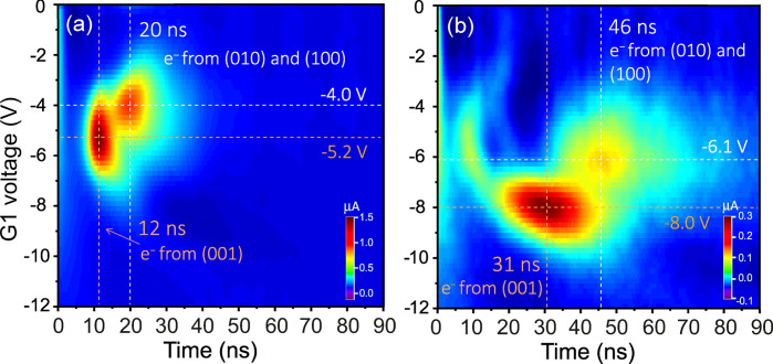
Experimentally observed time-resolved currents in a dual-gate transistor at 78 K. Drain currents at D1 (panel (a)) and at D2 (panel (b)) are shown, as a function of applied gate voltage (VG1) and the time after carrier injection. The same set of bias voltages used in the simulations has been applied in the experiment: Vsource = −7 V, VG2 = −2.4 V, Vbackplane = −2.4 V, with the drains grounded.
Our experimentally observed arrival times are within 8% of the values obtained from the simulation. The absolute values of the gate voltages at peak current are slightly underestimated in the simulation (5%–20%), which can be explained by the presence of interface states that are not taken into account in the simulation. The main difference between the experimental and the simulated data is that the peaks are broader experimentally. This is presumably due to small inhomogeneities in the electric field originating from extended defects, such as dislocation bundles.
In a second experiment, we use the electroluminescence (EL) from diamond NV centers to image the current density at the sample surface. This was done by introducing NV centers in a thin (120 nm) layer below the top electrodes via ion implantation, followed by an annealing step, as seen in Figure 1b. The layer makes it possible to optically monitor current densities using EL as the charge state of the NV center is affected by the presence of conduction band electrons.24 The rear surface was covered with a thin gold layer providing an optically semitransparent back contact, which provides a well-defined reference potential. The EL was observed through the sample and the semitransparent back contact using a home-built microscope equipped with a cooled sCMOS camera. More details on the device fabrication are given in section S2 in the Supporting Information. In this experiment, electron–hole pairs were generated near the source electrode by the 213 nm wavelength laser at a repetition rate of 660 Hz with short (800 ps) pulses with an energy of 10 nJ/pulse. Exposure times of several seconds ensured that enough light was collected to yield clear images. Figures 5b and 5c show how the observed EL shifts between different locations in the device just by varying the gate voltages. These images are composites with two different exposure times: 60 ms inside the dashed yellow circle and 8 s outside. The line inside the circle is strong luminescence from the region where electron–hole pairs were generated. EL was observed at D1 for VG1 = −9.6 V and VG2 = −5.2 V (Figure 5b), while it clearly shifted to D2 by changing the gate bias to VG1 = −13 V and VG2 = −7.0 V (Figure 5c). In Figures 5b and 5c, the EL spectrum comes from the rightmost part of the device (to the right of G2). The illuminated area was masked off so that light from this region did not enter the spectrometer and the measurements were integrated over time. The conduction band electrons that are generated by laser illumination are excited across the indirect band gap with a possible (many orders of magnitude smaller) contribution from photoionization of NV centers. The presence of a dominant 575 nm peak in the luminescence spectra, together with several phonon replicas (Figure 5d), show that the luminescence indeed originates from neutral charge (NV0) centers. The specific optical signature of the different charge states of NV centers has been discussed and identified in refs (12 and 25−27). The EL can be understood28 using a three-stage process:
(i)The NV0 center traps a conduction band electron and is converted to the negative charge state (NV–).
(ii)The NV– center reverts to the neutral state by detrapping the electron, either by direct tunneling to the contact or by hopping conduction via other defects, leaving the NV0 center in an excited state.
(iii)The NV0 center reverts to the ground state and emits a photon. The three stages are shown in the inset of Figure 5d.
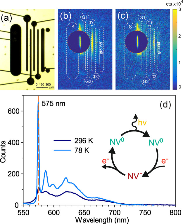
Electroluminescence (EL) from the valley pseudospin current. (a) Transmitted light optical micrograph of the transistor. (b,c) Luminescence images at 78 K for different gate voltages, of the transistor imaged in panel (a). The transistor is near the contact surface equipped with a thin layer of NV centers that luminesce with a typical NV0 spectral signature, with a strong zero phonon line (ZPL) at 575 nm at 78 K, together with associated phonon replicas, as shown in panel (d). For comparison, the room-temperature spectrum is also presented in panel (d). The spectrum is made with the leftmost part (left of G2) masked off. The position of the contacts are indicated in panels (b) and (c) by dashed white lines. Note the shift in EL from D1 to D2 as the gate bias is varied.
In summary, we have demonstrated electrostatic control of valley currents in dual-gate diamond field-effect transistors, as well as charge-state manipulation of NV centers. This was done by detecting different electron drift times in time-resolved current measurements and also by direct observation of electroluminescence from NV centers near the receiving contacts. Transport simulations of valley-polarized electrons show good agreement with the observations. These valleytronic devices enable electrostatic manipulation of valley currents and can be used to deliver electrons with a high degree of valley polarization for, e.g., electrical pumping of color centers in diamond for single-photon sources. They offer a possible solid-state platform for valleytronic-based information processing and for further investigations into the physics of spin-valley states. We anticipate that such devices will play a significant role in quantum information processing and future quantum computing.
The Supporting Information is available free of charge at https://pubs.acs.org/doi/10.1021/acs.nanolett.0c04712.
Monte Carlo simulations, sample processing, experimental details, detection of valley polarization in a parallel-plate configuration and additional luminescence images with experimental details (PDF)
J.I. designed the experiment. J.I., S.M., M.G., N.S., and K.K.K performed the measurements. J.I. provided the interpretation, and N.S. and V.D. performed the computer simulations. N.S., S.M., and K.K.K. prepared the samples, and D.J.T. and I.F. were responsible for sample CVD deposition. All of the authors discussed the results and gave input on the manuscript.
The authors declare no competing financial interest.
This study is supported by the Swedish Research Council (research grant No. 2018-04154), the ÅForsk Foundation (Grant Nos. 15-288 and 19-427), the Olle Engkvists Foundation (No. 198-0384) and the STandUP for Energy strategic research framework. The Monte Carlo simulations were performed on resources provided by the Swedish National Infrastructure for Computing (SNIC) through the Uppsala Multidisciplinary Center for Advanced Computational Science.
 A Valleytronic
Diamond Transistor: Electrostatic Control
of Valley Currents and Charge-State Manipulation of NV Centers
A Valleytronic
Diamond Transistor: Electrostatic Control
of Valley Currents and Charge-State Manipulation of NV Centers
 Facebook
 Twitter
 Linkedin
 Whatsapp
