
Studies of thermally induced transport in nanostructures provide access to an exciting regime where fluctuations are relevant, enabling the investigation of fundamental thermodynamic concepts and the realization of thermal energy harvesters. We study a serial double quantum dot formed in an InAs/InP nanowire coupled to two electron reservoirs. By means of a specially designed local metallic joule-heater, the temperature of the phonon bath in the vicinity of the double quantum dot can be enhanced. This results in phonon-assisted transport, enabling the conversion of local heat into electrical power in a nanosized heat engine. Simultaneously, the electron temperatures of the reservoirs are affected, resulting in conventional thermoelectric transport. By detailed modeling and experimentally tuning the interdot coupling, we disentangle both effects. Furthermore, we show that phonon-assisted transport is sensitive to excited states. Our findings demonstrate the versatility of our design to study fluctuations and fundamental nanothermodynamics.
Serial double quantum dot (DQD) devices are attractive systems for both fundamental quantum physics studies and quantum electronic-based applications with well-established charge transport properties.1−3 Because of the electronic structure4 and controllable level detunement, DQDs are highly sensitive to their environment. Consequently, interactions of DQDs with their charge environment, photons,5,6 and phonons7−17 have been demonstrated and used for frequency resolved noise, photon, and phonon detection.18−20
In this Letter, we study the impact of interactions between a DQD and its thermal environment on transport across the device. The relation between electrical transport and temperature gradients in nanoscale systems is important for applications as energy harvesters21−28 or fundamental studies of statistical physics.29−33 In a conventional setup, thermoelectricity is driven by the temperature difference created between electrical probes of a circuit which induces a current. Here, in addition to the thermoelectric effect (TE) across a DQD, we consider how a thermal reservoir decoupled from the electronic circuit of the device affects currents by phonon-assisted transport (PAT). We demonstrate how PAT and the TE can be unambiguously distinguished and used to probe excited states. Furthermore, we show experimentally that PAT can be used to harvest energy from the heated lattice in a three-terminal geometry, which is a concept proposed by Entin-Wohlman et al.34 and theoretically studied for a variety of related systems.35−39
Our experimental device is shown in Figure 1a. A DQD is epitaxially formed within an InAs nanowire via three InP segments.40,41 Plunger gates control the energy levels of the left and right quantum dot (QD) by applying a voltage VL(R) to the left (right) plunger gate. The DQD device is coupled to the thermal reservoirs in the contacts with electron temperatures TS and TD of the source and drain contact, respectively. Additionally, the lattice acts as third thermal reservoir with a phonon temperature Tph. A metallic joule-heater electrode in close vicinity to the nanowire, decoupled from the electronic system of the DQD, serves as an external heat source. By design, a current driven through the joule-heater by a heating bias dVH = |VH1 – VH2| heats the lattice more than the electron reservoirs of the DQD. A small misalignment of the electrode with the DQD structure in the nanowire further leads to an asymmetric impact on the contact electron temperatures.

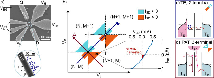
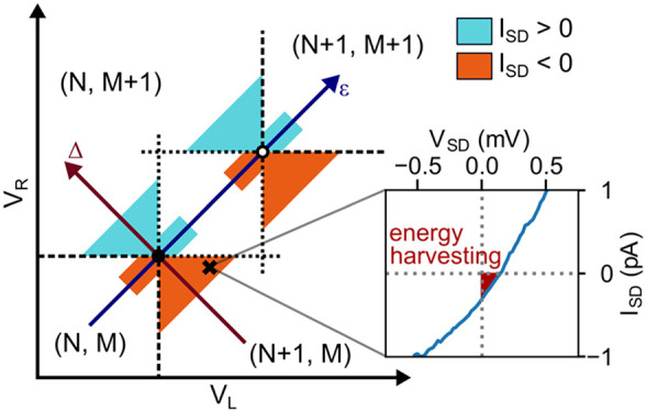
(a) Scanning electron microscope image of the device. An InAs/InP nanowire on a substrate acting as backgate (VBG) is contacted (S, D) and plunger gates (VL, VR) are placed in close vicinity to the DQD. The inset shows a transmission mode scanning electron microscope image of the nanowire. Three InP segments embedded in the InAs nanowire serve as tunnel barriers to epitaxially form a DQD. A heater electrode (VH1, VH2) is aligned with the DQD to heat the device. (b) Schematic illustration of temperature gradient driven currents in the charge stability diagram of DQD devices in the absence of external bias. Colored regions illustrate where currents are induced by the TE or PAT for the case Tph > TS > TD around the (N, M) → (N + 1, M + 1) transition. Inset: Experimental six-time averaged ISD–VSD curve, measured with a heating bias of dVH = 4 V at a point corresponding to the black cross in the charge stability diagram. The offset of the curve toward the origin indicates that the device produces power. (c) Schematic illustration of the TE, inducing transport along the energy axis ϵ = μ – (EL + ER)/2. (d) Schematic illustration of PAT along the level detunement axis Δ = EL – ER. The insets in (c,d) show the characteristic current patterns around the TP and the white crosses indicate the location of the level combinations shown in the panel.
In the following, we describe the device as a DQD with small interdot tunnel coupling Ω, that is weakly coupled to the source and drain electron reservoirs. Figure 1b illustrates the charge stability diagram of the DQD in plunger gate space around a pair of triple points (TP) in the (N, M) → (N + 1, M + 1) charge transition region. The black and white dots label the position of electron and hole TPs, respectively. Here, we assume that due to substantial charging and level-quantization energies only a single level with energy EL/ER can be additionally occupied in the left/right dot containing already N/M electrons in this region. These addition energies are essentially linear functions of the gate voltages EL/R = αL/R(VL/RT – VL/R), where VL/RT are the voltages at the electron triple point and αL/R are the lever arm factors. For the sake of convenience, we define local coordinates ϵ = μ – (EL + ER)/2 and Δ = EL – ER, where μ = μS = μD is the chemical potential for vanishing source-drain bias VSD = 0 V. Charging lines separate regions of different overall charge (dashed lines) and upon crossing the charge transfer line, connecting the two TPs along ϵ, an electron is transferred from one QD to the other. In the absence of photons, phonons, or a driving bias voltage, no net current flows and conductivity is only expected on the TPs. Cyan (orange) shaded areas indicate where heating the device via the joule-heater electrode can drive positive (negative) currents in the absence of a voltage bias.
The TE illustrated in Figure 1c occurs when TS ≠ TD. The effect manifests along the axis ϵ when levels in each QD are aligned and moved in energy together. The applied temperature gradient causes different energy distributions of the electronic reservoirs around the electrochemical potentials μ. The DQD connecting the two reservoirs acts as an energy filter probing the electron population imbalance at a set energy.42 For ϵ < 0 (ϵ > 0), this causes electrons to flow from hot to cold (cold to hot). Consequently a reversal of the thermoelectric current polarity is observed upon crossing each TP along ϵ. This effect has been studied in single QD devices26,42−47 as well as in DQDs.48
PAT via phonon absorption is an inelastic transport mechanism requiring a detuned two-level system. Along the energy axis, Δ = EL – ER levels on the two QDs are energetically detuned, as illustrated for Δ > 0 in Figure 1d. For large Δ, thermoelectric currents are blocked. Electrons can then only be transported from the energetically lower occupied to the higher unoccupied energy level of the DQD by absorbing a phonon from the hot phonon bath, and a net current can flow if Tph > TS, TD.49 Reverting the sign of Δ (crossing the charge transfer line where Δ = 0) causes the electron transport to revert direction. Consequently, PAT yields currents of opposite polarity on opposite sides of the charge transfer line as long as the spectral distribution of the phonon bath provides sufficient phonon energies to overcome the DQD level detuning. For |Δ| ≫ kBTph, this condition is no longer fulfilled and PAT is suppressed. We note that a significant difference in occupation between the initial and final state for the PAT process is required.49 Without external bias, this requirement is only fulfilled if the two involved states are on opposite sides of the Fermi surface. Thus, PAT active regions are limited to triangular areas within the charge stability diagram as shown in Figure 1b.3,8
Within these active regions, it is possible to harvest energy from an external heat source, as demonstrated in the inset of Figure 1b. Successful operation of our device as a three-terminal energy harvester at dVH = 4 V is evident by the nonzero current ISD at VSD = 0 V. Considering R ≈ 1 MΩ in series with the device, as used for this measurement, we extract a power of P = RISD2 ≈ 0.1aW.26,50 In the limit of weak tunnel couplings, this translates to an upper bound for the unoptimized efficiency of the electronic system, η = P/QH = (RISDe)/Δ = 0.03%.24 Here, the heat flow QH = ΔISD/e describes the energy gain of the detected electrons upon phonon absorption.
To experimentally study heat driven currents in our device, we first characterize the DQD via conventional finite bias spectroscopy and pick a range in the intermediate (Figure 2a) and weak (Figure 2b) interdot coupling regime. Details of the device characterization and measurement conditions are given in the Supporting Information (SI).
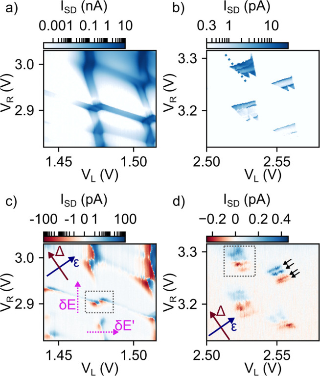
(a) Bias driven current ISD as a function of the plunger gate voltages VL and VR at VH1 = VH2 = −4 V, VBG = 0 V and VSD = 1 mV in the intermediate interdot coupling regime. (b) Bias driven current ISD in the weak interdot coupling regime withVH1 = VH2 = −4 V, VBG = −1 V and VSD = 3 mV. (c) Experimental heat driven current ISD as a function of the plunger gate voltages measured at VSD = 0 V and dVH = 1 V in the intermediate interdot coupling regime. The current is plotted on a logarithmic scale with a linear range between ±1 pA. (d) Experimental heat driven current ISD, measured at VSD = 0 V and dVH = 4 V in the weak interdot coupling regime. Dotted, gray rectangles in (c,d) label a comparable small range around a single set of TPs as in Figure 1b.
We now demonstrate a key capability of this study: By controlling the interdot tunnel coupling, we tune the dominant mechanism behind thermally driven currents between the TE and PAT. Figure 2c,d presents exemplary measurements of purely thermally driven currents ISD across a heated DQD as a function of the plunger gate voltages VL and VR in the intermediate (c) and weak (d) interdot coupling regimes. These measurements effectively map heat driven transport signals within the DQD charge stability diagram. While maintaining Tph > TS > TD in both measurements, we experimentally find apparent differences in heat driven transport in the intermediate and weak interdot coupling regimes. A detailed characterization of the signals at different heating bias dVH is given in the SI.
In the intermediate interdot coupling regime (Figure 2c), the pronounced polarity reversal of current close to the TPs occurs along the energy axis ϵ, suggesting the thermoelectric effect to be the main transport mechanism. Further, signals also appear along the charging lines and are in good agreement with thermoelectric transport across an intermediately coupled DQD observed by Thierschmann et al.48 In contrast, in the weak interdot coupling regime (Figure 2d) currents reverse the sign perpendicular to ϵ, along Δ, which is characteristic for a PAT dominated system. With the exception of pronounced resonances (black arrows), our results qualitatively match previous studies on phonon-mediated back action of charge sensors on transport through weakly coupled DQDs.8,11,12,15
To explain the difference between the intermediate and weak interdot coupling regime, we consider the impact of the interdot tunnel coupling Ω on heat driven transport. Discrete energy levels EL and ER confined to the left and right QD respectively only exist for Δ ≫ Ω when mixing effects are suppressed.18 In contrast, if Δ ≫ Ω is not fulfilled, the electronic wave functions will extend over both QDs, and mixing of EL and ER leads to the formation of bonding and antibonding molecular states Ebond, Eantibond.51 The molecular states are energetically separated by

For PAT, the formation of bonding and antibonding molecular states introduces new, additional constraints as phonons now have to supply a minimum energy of Eph > 2Ω even at small Δ, which agrees with observations in photon-assisted transport experiments.52 Consequently, the onset of PAT is offset toward higher phonon energies and temperatures with increasing Ω. In addition, as a result of the electronic wave functions extending across both QDs51 the directionality of PAT is reduced as electrons now have an increased probability to tunnel back into their initial reservoir and not contribute to the detected PAT current signal. The thermoelectric effect on the other hand benefits from the formation of molecular states. Although for Δ ≫ Ω, elastic thermoelectric transport is blocked, for large Ω this blockade is lifted due to the extended wave functions, and thermoelectric current contributions can be observed in an increased range along Δ. Finally, along the more horizontal (vertical) charging lines where a level in the right (left) QD is aligned with μSD, the DQD behaves as single QD with an effective left (right) tunnel coupling ΓL(R),eff ≈ ΓL(R)Ω2/Δ2.53 As a result of the high Ω, currents are observed along these charging lines in the heated case which along an energy axis δE (δE′) resembles a pure TE across a single QD because no final state for a PAT process is available.
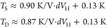
We use the observation of pure TE signals along the charging lines in the intermediate interdot coupling regime to estimate contact electron temperatures TS/D independently of the phonon temperature and find
In order to disentangle the individual TE and PAT contributions to the experimental signal further, we performed detailed simulations of the transport through a DQD system with two spin degenerate levels in each QD (ground levels EL/R and excited levels with spacing ΔEL = 0.8 meV and ΔER = 1.7 meV). Furthermore, we use the Coulomb interaction terms for intradot U = 8 meV, for interdot Un = 1.4 meV, and for intradot exchange Uex = 0.4 meV. These parameters are motivated in the SI, where additional simulation details are given. All transport simulations are done with the open source simulation tool QMEQ [Quantum Master Equation for Quantum dot transport calculations]54 with the recent inclusion of phonon scattering.49 To model the side-heating, we assume the phonon temperature
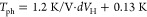
Figure 3a,e shows simulation results for a fixed VSD = 1 mV without heating. For the weak interdot coupling case (upper panels), the current shows distinct triangles around the triple points. Instead, for the simulated intermediate interdot coupling case (lower panels), anticrossing behavior is visible and is qualitatively in agreement with the experimental data in Figure 2a. With heating, the panels (b,f) correspond to, and qualitatively agree with the gray rectangles in Figure 2c,d and show the typical pure heat driven current distribution due to combined PAT and TE currents for Tph > TS > TD. In the simulations, we are able to disentangle both effects by separate modification of the temperatures. In panels (c,g), the PAT contribution is removed by setting the phonon temperature as the mean of temperatures in the source and drain contact. Here, we obtain a current profile, where the sign changes only along the axis ϵ in vicinity to the TPs. In the intermediate interdot coupling regime, signals further extend along the charging lines. In contrast, if we remove the TE contribution by assuming Tph > TS = TD, see Figure 3d,h, the pure PAT current reverses polarity along the Δ axis near the TPs exclusively.
Simulated charge stability diagram around the (0,1) → (1,2) charge state transition in the weak (a–d) and intermediate (e–h) interdot coupling regime. (a,e) Finite bias spectroscopy at VSD = 1 mV, dVH = 0 V and TS = TD = Tph = 130 mK. Heat driven currents are simulated at VSD = 0 mV and dVH = 1 V in the weak (b–d) and intermediate (f–h) interdot coupling regime. (b,f) Temperatures Tph, TS, and TD are set using eqs 2 and 3. In (c,g) Tph is replaced by the average of TS and TD, whereas in (d,h) we use TS = TD = 0.9 K/V·dVH + 130 mK and Tph is set by eq 3.
In the weak coupling regime, thermoelectric currents are an order of magnitude smaller than PAT currents (compare Figure 3c,d). This is a result of the PAT driving temperature difference Tph – TS growing faster with dVH compared to the difference TS – TD driving the TE. Consequently, the mixed signal in Figure 3b appears almost exclusively PAT-like. In contrast, in the intermediate coupling regime PAT is suppressed and the TE benefits from the increased interdot coupling. The TE and PAT contributions here, see Figure 3g,h, are of comparable magnitude for the chosen dVH = 1 V and the mixed signal in panel (f) shows a complex superposition as observed in the experiment.
Finally, we return to weak interdot coupling and address the pronounced resonances within Figure 2d (black arrows), which were not observed by previous PAT or thermoelectric effect related studies. Comparable features are reported for experiments based on photon-assisted transport across DQDs and are attributed to multiphoton processes.5,52 In contrast to those experiments, we find the resonances in Figure 2d (and SI) to be asymmetric with respect to the charge transfer line. This asymmetry, in combination with the continuous PAT signal along Δ, rules out resonant one- and two-phonon processes. To study the origin of the resonances, we combine finite bias spectroscopy with heated measurements.
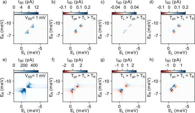
Figure 4a shows the current ISD without heating, dVH = 0 V, as a function of VSD along the cut-line Δ, marked by a blue dotted line in Figure 2b. The cut-line is chosen such that it crosses finite bias triangles forming in both positive and negative VSD direction. We note that the observed linear slope of the groundstate (GS) to groundstate transition line (the charge transfer line), where the energetically lowest available state in each QD mediates transport, is an effect of the source contact’s capacitive coupling to the DQD. Δ is manually set to zero where the charge transfer line intersects with VSD = 0 V. For positive (negative) VSD we detected how the finite bias triangle grows in height with negative (positive) Δ. Sudden changes in current are observed when a new excited state (ES) becomes available for transport and is initially aligned with the GS in the other QD. This allows mapping of the GS–ES spacing for the left (Δ < 0) and right (Δ > 0) QD. The values for the GS–ES spacings in millielectronvolts are annotated in Figure 4a. For positive VSD, an additional GS–ES spacing of 1.7 meV (labeled by *) is obtained from Figure 2b. We note that the current suppression before the triplet state becomes available (below 1.4 meV) within the finite bias triangle for negative VSD is Pauli spin blockaded.55−57 The spin blockade is lifted along the GS–GS transition, possibly due to hyperfine- or spin–orbit-interaction.58 Further, the change in slope of the triangle outline for VSD > 0 and Δ < −0.8 meV is a result of the chosen cut-line position which ceases to overlap with the triangle.
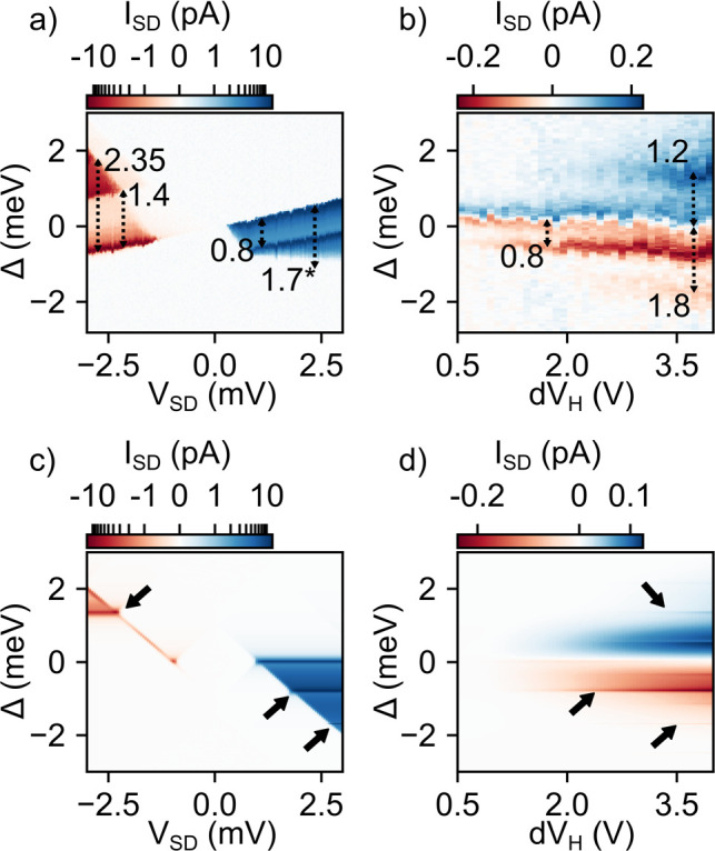
(a) Current measurement along the cut-line Δ (blue dotted line in Figure 2b) as a function of the driving bias VSD at dVH = 0 V. The current is plotted on a logarithmic scale with a linear range between ±1 pA. (b) Current along Δ as a function of the heater voltage bias dVH at VSD = 0 V. Numbers in (a) and (b) correspond to the energetic spacing from resonance to the charge transfer line in millielectronvolts, indicated by dotted black arrows. The excited state at 1.7 meV (labeled by * in (a)) is slightly outside the overlap of the cut-line with the bias triangle and the spacing is read out from Figure 2b. Each data point in (a) and (b) is the result of two-time averaging. (c) Simulation of (a) at Tph = TS = TD = 130 mK. (d) Simulation of (b) using the temperature calibrations given in eqs 2 and 3. Black arrows in (c,d) label energetically matching resonances within the bias and heat driven simulated currents.
Figure 4b shows the current ISD along the cut-line Δ as a function of dVH for VSD = 0 V. The PAT-induced current polarity reversal at Δ = 0 is clearly visible. With increasing dVH, the phonon temperature Tph increases, which provides larger currents. Furthermore, the PAT currents are visible for |Δ| being less than a few kBTph, as phonons with higher energies are entirely frozen out. Thus, the PAT active regions grow with increasing dVH. Resonances, as observed in Figure 2d, begin to appear with increasing heating voltages dVH. The energy spacing in millielectronvolts from resonance to charge transfer line is annotated in Figure 4b, and we find similar values to the GS–ES spacings in Figure 4a.
One possible cause for the resonances is a TE through aligned GS–ES configurations. This would lead to a polarity reversal of the current on the resonances once the aligned GS–ES levels are energetically pulled below μ as we follow the resonance in direction of ϵ. We interpret the absence of this polarity reversal in Figure 2d as an indication of PAT through excited states as origin for the resonances.
To confirm a PAT process as the origin of the resonances, we simulate the bias and purely heat driven currents along a cut-line Δ = EL – ER – Δ0 in Figure 4c,d, corresponding to the experiments in Figure 4a,b. Here, for EL = ER + Δ0 the ground states GS(1, 1) and GS(0, 2) are in resonance. For biased transport, in Figure 4c spin blockade is observed until the triplet ES(0, 2e) gets in resonance with GS(1, 1) for negative VSD but in contrast to the experiment no partial lifting by hyperfine- or spin–orbit interaction is considered.
By comparison of Figure 4c,d to their experimental counterparts, we first find good qualitative agreement. Second, we identify matching resonances in Figure 4c,d, labeled by black arrows and identify the relevant transport mechanism in the simulations as PAT through excited states. A detailed identification of the different transitions responsible for the current peaks is given in the SI.
In summary, we present a detailed, combined experimental and theoretical study of heat driven transport in a DQD coupled to three thermal reservoirs. We show how via tuning the interdot tunnel coupling, the dominant transport mechanism can be tuned between the two-terminal TE and three-terminal PAT, which is further found to be sensitive to excited states. Consequently, we demonstrate the applicability of conventional DQD devices as highly versatile and controllable energy harvesters and provide a platform and the tools to conduct and analyze fundamental nanothermodynamic experiments.
General conclusions about the performance and ideal operating conditions of our device as an energy harvester are complex to draw due to the high degree of freedom and require knowledge of the phonon spectral function to accurately determine Tph. Conceptually similar systems have in that regard been only theoretically analyzed.38,59 We thus consider future experiments combining access to the phonon spectral function17 with a dedicated study of the energy harvesting performance of our system as highly interesting.
The Supporting Information is available free of charge at https://pubs.acs.org/doi/10.1021/acs.nanolett.0c04017.
Device fabrication and measurement details including finite bias spectroscopy, bias offset characterization, contact electron temperature estimations, detailed characterization of the heat driven current signal in the weak and intermediate interdot coupling regime as well as simulation details, analysis of tunnelling via excited states, and further simulations (PDF)
The authors declare no competing financial interest.
The authors thank H. Linke for fruitful discussions and acknowledge funding by the Knut and Alice Wallenberg Foundation (KAW) (Project 2016.0089), the Swedish Research Council (VR) (Project 2015-00619), the Marie Skłodowska Curie Actions, Cofund, Project INCA 600398 and by NanoLund. Device fabrication was carried out in the Lund Nano Lab (LNL), and computational resources were provided by the Swedish National Infrastructure for Computing (SNIC) at LUNARC.
 Heat Driven Transport in Serial Double Quantum Dot
Devices
Heat Driven Transport in Serial Double Quantum Dot
Devices
 Facebook
 Twitter
 Linkedin
 Whatsapp
