
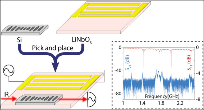
The rapid development of quantum information processors has accelerated the demand for technologies that enable quantum networking. One promising approach uses mechanical resonators as an intermediary between microwave and optical fields. Signals from a superconducting, topological, or spin qubit processor can then be converted coherently to optical states at telecom wavelengths. However, current devices built from homogeneous structures suffer from added noise and a small conversion efficiency. Combining advantageous properties of different materials into a heterogeneous design should allow for superior quantum transduction devices—so far these hybrid approaches have however been hampered by complex fabrication procedures. Here we present a novel integration method, based on previous pick-and-place ideas, that can combine independently fabricated device components of different materials into a single device. The method allows for a precision alignment by continuous optical monitoring during the process. Using our method, we assemble a hybrid silicon–lithium niobate device with state-of-the-art wavelength conversion characteristics.
Hybrid photonic devices have attracted significant attention for their potential in both classical and quantum information processing.1−4 While individual materials rarely possess all desired properties, the combination of several materials allows for superior designs needed for the realization of photonic circuits that include light generation, guiding, modulation, and detection. For example, the integration of silicon photonic circuits with single photon sources,5 two-dimensional materials,6 and classical light sources7 has been demonstrated, promising new capabilities beyond what is achievable with a homogeneous approach. This optimization and combination of several desired properties often comes at the expense of significantly more complex fabrication procedures, complicating the development of more advanced hybrid photonic devices. Different material systems typically react differently to chemicals or etching procedures, leading to incompatibilities in the fabrication process. Here we present a novel approach to the fabrication of hybrid devices, based on a “pick-and-place” procedure, which is agnostic to the photonic material and compatible across a large range of different platforms. Additionally, this technique can use in situ alignment to achieve accurate positioning without a complex imaging system. We demonstrate the capabilities of our new method by combining a silicon photonic crystal cavity with a piezoelectric lithium niobate transducer and experimentally demonstrate state-of-the-art microwave-to-optics wavelength conversion. Coherent conversion of quantum states between optical and microwave frequencies through a quantum transducer has become an attractive candidate to connect superconducting quantum processors. Though well-suited for local manipulation, the low frequency of superconducting circuits makes processors in distant cryostats difficult to connect.8,9 A quantum transducer can solve this issue by converting quantum information into the optical domain, where it is protected against room-temperature thermal noise.10,11 Low-loss optical fibers can then be used to transmit information over large distances, creating a network of connected quantum processors.12,13
In particular, electro-optomechanical devices have emerged as a leading platform for realizing quantum transducers.14−25 In such a device, an optomechanical interaction is used to transfer quantum excitations between optical and mechanical modes,4,26 while a resonant electromechanical (often piezoelectric) drive can be used for efficient conversion between mechanical and microwave modes.27 The manipulation of a quantum state of the mechanical resonator at the single phonon level has been demonstrated with both optomechanical28−30 and piezoelectric interactions.31−33 Most recently, photons from a microwave qubit have been converted into telecom photons25 using a hybrid aluminum nitride-on-silicon-on-insulator platform. While these first proof-of-principle experiments are highly encouraging, further improvements to the efficiency and fidelity will require even stronger piezoelectric materials.
On the one hand, state-of-the-art quantum optomechanical experiments primarily use silicon due to its high refractive index and photoelasticity, which enable large optomechanical coupling rates, as well as its small optical absorption. On the other hand, some of the most promising candidates for facilitating efficient coherent interactions between microwaves and mechanics are highly piezoelectric materials like LiNbO3 and AlN.19,23,25 Therefore, combining silicon photonics with these piezoelectric materials into a single hybrid electro-optomechanical device naturally emerges as an attractive approach to establish a coherent link between microwave and optical modes.34 Single-material (or homogeneous) approaches have been investigated,21,23 but currently they suffer from a lack of a material that fulfills the requirements for both strong piezoelectric and optomechanical coupling. To avoid this problem, optomechanical wavelength converters can use a hybrid approach,25 where a device is fabricated from multiple materials. However, this often comes at the expense of a more complex nanofabrication procedure.
In this work, we present a simple, flexible strategy for realizing such devices. We use a pick-and-place technique3 to assemble a hybrid structure from components fabricated on separate chips. A wavelength converter requires a high degree of accuracy in assembly to reach the maximum efficiency. We develop a method that can achieve state-of-the-art nanoscale positioning with a straightforward procedure. Working with only a simple micropositioning stage, a microscope, and a digital camera, we utilize a tapered optical fiber to transfer a silicon photonic device onto a piezoelectric chip (cf. Figure 1). Replacing commonly used tungsten tips with a tapered fiber enables one to use the photonic cavity’s evanescent field as a high-precision position sensor. The simplicity and flexibility of the technique makes it well-suited for the development of novel devices, previously only possible through difficult and lengthy fabrication procedures, as well as proof-of-principle experiments with almost any combination of materials. Unlike wafer-scale bonding approaches, pick-and-place techniques enable a straightforward approach to the further integration of electro-optomechanical devices with other quantum technologies without significantly changing fabrication procedures. This material-independent technique is useful for rapid prototyping and integrating new material combinations in hybrid photonic circuits. Though the surface interaction between certain materials might prevent an integration as straightforward as the one demonstrated here, it is possible to mitigate this issue by modifying the surface of the chip. Our technique is an especially attractive approach for coupling cavities to single-photon sources, as the measurement of coupling during the placement can enable an optimal positioning of the cavity. We illustrate the capabilities of our new technique by demonstrating a silicon photonic crystal cavity combined with a LiNbO3 electromechanical system, previously a difficult-to-realize material combination. We further experimentally characterize the device and demonstrate its potential for quantum transduction tasks.

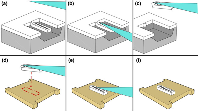
Slapping: Pick-and-place assembly with tapered optical fibers. A cartoon depiction of the “slapping” procedure. (a) Photonic crystal nanobeams are patterned in a thin film of silicon (white) released from a thick oxide layer (gray). (b) A tapered optical fiber (cyan) touches the nanobeam and sticks due to van der Waals forces. (c) The thin tether of silicon connecting the nanobeam to its chip is broken through repeated motion with the fiber, and the photonic device is lifted away. (d) The fiber and nanobeam are brought into close proximity with the substrate of a different chip (yellow). The optical and mechanical spectra of the nanobeam can be measured in order to map the surface and locate an optimal placement location (indicated by the red outline), in principle creating the possibility to align to various defects, such as spins, in the new material. (e) The nanobeam is then touched down onto the surface. (f) Once the device is properly assembled, the fiber is lifted.
Several quantum transducers using thin-film lithium niobate have shown promising results,19,20,23 due to the large values of the material’s piezoelectric tensor. However, these homogeneous approaches failed to achieve the high optomechanical coupling necessary for efficient transduction, as LiNbO3 has a relatively small refractive index (nLN ≈ 2.2 at 1550 nm). By incorporating a silicon cavity the optomechanical coupling of a thin-film lithium niobate device can be significantly increased. In our approach, the transducer is assembled by placing a one-dimensional silicon photonic crystal nanobeam on top of a suspended lithium niobate membrane patterned with electrodes used for piezoelectric coupling (see Figure 2a). This hybrid structure supports mechanical modes that are distributed across both materials and that couple to both optical and microwave electromagnetic fields. The membrane resonator is made from X-cut lithium niobate and is designed to support gigahertz-frequency Lamb wave modes along the y-axis of the crystal, as shown in Figure 2b. Through finite-element simulations, we find A0-like modes (zeroth-order asymmetric Lamb wave), where the stress inside the silicon nanobeam closely resembles the stress distribution of its breathing mode35 (cf. Figure 2c). A higher piezoelectric coupling can be expected for S0-like modes, albeit with lower mechanical quality factor due to the geometry of our device. The mechanical modes of the membrane are excited by an array of equally spaced electrodes, known as an interdigital transducer (IDT). The pitch of the electrodes determines the frequency of the excited modes, while the number of fingers sets the bandwidth.36 Using a large membrane with large number of IDT fingers will lead to higher coupling rates between mechanical modes and microwaves, but this comes at the expense of a reduced optomechanical coupling, as more effective mass is added to the mechanical mode. We design our electromechanical device with two finger pairs and dimensions of 0.34 × 5.4 × 15 μm, with a pitch of 1.5 μm. From finite-element simulations, we expect an effective electromechanical coupling coefficient keff2 ≈ 1% for our membrane design.
![Hybrid
piezo-optomechanical devices. (a) A false-color SEM image
of a LiNbO3 film acoustic resonator with a silicon photonic
crystal cavity placed on top. The released LiNbO3 is light
gray, the silicon nanocavity is blue, the gold electrodes are yellow,
and the lithium niobate marker used for positioning is purple. The
silicon cavity features a tapered waveguide that is used for coupling
light from an optical fiber (not shown). (b) Simulated strain component syy, which is dominant for photoelastic and piezoelectric
coupling. Shown is the profile of a mode of the hybrid device, top
view (left) and cross-section with the mechanical deformation (right).
(c) Fundamental resonant optical mode of the silicon photonic crystal
cavity nanobeam, viewed from the top. The indicated axes correspond
to the lithium niobate axes, while the silicon nanobeam is fabricated
from a [100] wafer, with the cavity along the [110] direction.](/dataresources/secured/content-1765769105614-0ed7cc7d-f6ed-4c8f-ad47-804deb56e5d8/assets/nl0c03980_0002.jpg)
Hybrid piezo-optomechanical devices. (a) A false-color SEM image of a LiNbO3 film acoustic resonator with a silicon photonic crystal cavity placed on top. The released LiNbO3 is light gray, the silicon nanocavity is blue, the gold electrodes are yellow, and the lithium niobate marker used for positioning is purple. The silicon cavity features a tapered waveguide that is used for coupling light from an optical fiber (not shown). (b) Simulated strain component syy, which is dominant for photoelastic and piezoelectric coupling. Shown is the profile of a mode of the hybrid device, top view (left) and cross-section with the mechanical deformation (right). (c) Fundamental resonant optical mode of the silicon photonic crystal cavity nanobeam, viewed from the top. The indicated axes correspond to the lithium niobate axes, while the silicon nanobeam is fabricated from a [100] wafer, with the cavity along the [110] direction.
The silicon nanobeam optical cavity on top of the membrane is formed by a photonic crystal mirror at each end and a tapered defect region in the middle,37 made out of 250 nm thick silicon. Finite-element simulations of the bare silicon photonic crystal cavity nanobeam show a fundamental resonance around 1565 nm with a quality factor exceeding 2 × 10⁵. When the nanobeam is placed on top of the LiNbO3 membrane its resonance is shifted to ∼1595 nm (see Figure 2c for details). We further calculate an optomechanical coupling rate of 24 kHz for an optimally positioned nanobeam.
We fabricate the lithium niobate devices using two electron-beam lithography steps. The first places electrodes on top of the membrane, and the second etches into the lithium niobate. The silicon nanobeam is fabricated in a single lithography step, with the photonic crystal cavity connected with single narrow bridge to the rest of the chip in order to be able to pick it up with the fiber during the transfer procedure (see the Supporting Information for more details).
Our approach for making hybrid photonic integrated circuits is based on the pick-and-place method, where structures are removed from a “donor chip” made of a desired material and are transferred to a “device chip” made of a traditional photonic material. In the past, this transfer has been accomplished using polymer stamps,38,39 atomic force microscopy (AFM) tips,40 or tungsten nanomanipulator probes.5,41−45 In contrast, we developed a new method using an optical fiber, which we refer to as slapping. One of the major advantages of our approach is that we can achieve high-precision positioning without sacrificing the ease of operation, because the silicon photonic devices can be directly and continuously measured during the transfer process.
Tapered optical fibers are commonly used to couple light into nanophotonic devices with high efficiency46−48 and have also been used to rip away loosely connected photonic crystal cavities from the chip they were fabricated on.49,50 Here, we extend this technique by placing the cavities onto a different substrate to create a hybrid photonic device. In our procedure (cf. Figure S3), silicon photonic crystal cavity nanobeams are attached by a thin tether (∼50 nm) on a donor chip. The chip is placed on a piezo-controlled motorized stage, where it is viewed from above through a 500× microscope objective using a charge-coupled device (CCD) camera. A tapered fiber is placed above the donor chip at an angle of a few degrees lower than horizontal, such that the tip is nearly parallel to the surface of the donor chip. The motorized stage is then used to touch the waveguide of a photonic crystal cavity using the tapered fiber, and van der Waals forces cause the fiber to adhere to the silicon. At this point, the optical and mechanical spectra of the optomechanical nanobeam can be measured with a tunable laser and photodetector using the reflected light in the optical fiber. This measurement can be used to preselect photonic structures supporting high-quality optical and mechanical modes, increasing the yield of the final devices.
Once the fiber is stuck to the nanobeam, the stages can be moved back and forth by a few microns, until the tether brakes and the nanobeam is ripped away. The donor chip is then lowered away from the fiber, and the device chip is moved into its place. The fiber is brought close to the surface of the device chip such that the silicon nanobeam and lithium niobate membrane are in focus simultaneously. A rough alignment can be done using the camera and microscope. With the evanescent field of the cavity, the environment surrounding the nanobeam can be probed, and its position with respect to the substrate can be determined. To further improve the accuracy of this alignment we include a thin marker in the LiNbO3 layer near the mechanical resonator (see Figure 2a). By moving the nanobeam over this marker and monitoring the optical spectrum a sharp reduction in the quality factor of optical modes due to scattering in close proximity to the marker can be observed (cf. Figure S4). Using this strategy, we are able to position the center of the optical cavity directly over the marker before transferring it to the mechanical resonator, which results in reliably placing our nanobeams with an accuracy of less than 100 nm, which is significantly better than what is possible with optical imaging methods. The angular alignment accuracy is typically ≪1°. Additional reduction in the alignment error can easily be realized through contact sensing and monitoring of the mechanical resonance of the cavity.
Once positioned, the fiber is then lowered, until the nanobeam touches down onto the membrane. As the van der Waals force makes the nanobeam stick to the substrate more strongly than to the fiber, the fiber can be lifted away from the hybrid structure. A finalized device using this method is shown in Figure 2a. We note that this technique is not material-specific and only uses materials typically used in a laboratory capable of optical characterization.
After assembly, we measure the microwave and optical reflection spectra of our devices, which were all patterned with the electrodes wired to large pads in a ground-signal-ground (GSG) configuration. We measure the signal in reflection using a coaxial radio frequency (RF) GSG probe and a vector network analyzer (VNA), and the signal is normalized to the open response of the probe.
For our full procedure, we first characterize the lithium niobate resonator before slapping the silicon nanobeam by measuring the microwave reflection spectrum. Prominent dips in the reflection spectrum (see Figure 3) indicate a power transfer into the mechanical modes of the device. After the slapping, the same measurement reveals that the resonances are slightly shifted, while the quality factors experience a modest decrease (Figure 4b, red trace). We observe groups of modes spaced by ∼330 MHz, which matches the free spectral range of the A0-like mechanical modes in our simulations. Optical spectroscopy of the hybrid device is performed using a tunable external-cavity diode laser. The reflection spectrum of the device shows two prominent resonances at 1588 and 1617 nm with a line width of 6.6 and 11.3 GHz, respectively (Figure 4a).
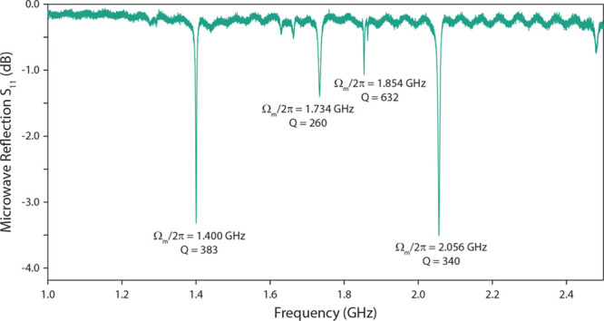
Characterization of a piezo-mechanical device before slapping. Electromechanical reflection spectrum of a fabricated lithium niobate device before the slapping procedure. The frequency and quality factor of four significant modes are indicated. After the slapping, the mode frequencies shift slightly, and the mode line widths change (cf. Figure 4).
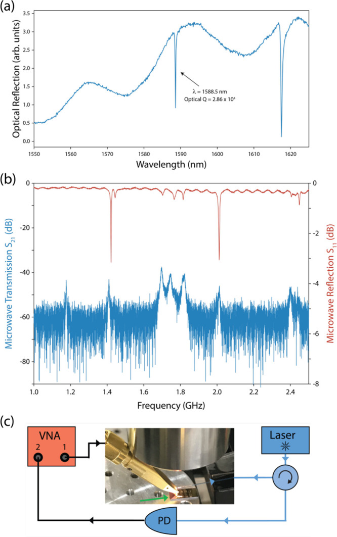
Microwave-to-optical transduction using a slapped Si-on-LiNbO3 device. (a) Optical reflection spectrum. (b) Full microwave reflection (S11, red) and transmission (S21, blue) signals as a function of frequency. The microwave transmission response of the device is proportional to its microwave-to-optical transduction efficiency. (c) Diagram of the experimental setup used to characterize the transduction of the device (indicated by the green arrow). PD, photodiode; VNA, vector network analyzer.
We then proceed to measure microwave-to-optical transduction at room temperature. A microwave tone is swept over the device, exciting the mechanical supermodes of the hybrid nanobeam-and-membrane structure on resonance. At the same time, optical laser light detuned to the blue side of the cavity by 1.4 GHz is continuously pumped into the nanobeam, through an optical circulator and a tapered optical fiber. On resonance, the mechanical motion excited by the microwave signal will drive the optomechanical Stokes process and create a sideband resonant with the optical cavity. The optical intensity resulting from the beat note between the reflected cavity and pump photons can be measured by monitoring the light reflected from the cavity on a fast photodiode. Key parameters such as single-photon optomechanical coupling rate g0 and microwave-to-optical efficiency ηeo can be extracted by comparing the response of the output of the fast photodetector to the microwave input. Using a VNA yields a transmission-type S21 measurement of microwave-to-optical transduction (Figure 4b, blue trace).
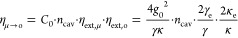
We select the mechanical mode at 1.7 GHz as our mechanical resonance, as it has the highest value in our S21 measurement. The input optical power sent into the cavity through the tapered fiber is Iin = 25.3 μW, while the overall received optical power at the photodiode is Irec = 804 nW. Following reference,19 the single-photon optomechanical coupling rate g0 can be extracted from the S21 in the sideband resolved regime, where we use Rload = 50 Ω for the impedance of the VNA ports and RPD = 1300 V/W as the responsivity of the photodiode. In our case the anti-Stokes sideband is not completely suppressed, leading to a slight under-estimation of g0. The microwave-to-optical transduction efficiency ημ→o is the product of the single photon cooperativity C0, the intracavity photon number ncav, and the microwave and optical external coupling efficiencies (ηext,μ and ηext,o, respectively)
We find g0/2π ≈ 10 kHz, which matches well with the simulated value of 13 kHz for a slightly nonoptimally placed nanobeam. While the large loss rates of the optical and mechanical resonators of 6.6 GHz and 12 MHz, respectively, keep this device out of the Concav > 1 regime, the relatively high external coupling efficiencies result in a photon number conversion efficiency of ημ→o ≈ 1 × 10⁻⁷ at an optical power of Iin = 25 μW in the fiber. This result is on par with homogeneous state-of-the-art LiNbO3 devices.19,23 On the one hand, while ref (19) exhibits a large microwave-to-mechanics conversion γe/γ = 0.15, it suffers from a small optomechanical coupling g0/2π = 1.1 kHz. On the other hand ref (20) utilizes small mode volume nanobeam cavities to achieve g0/2π ≈ 80 kHz but at the expense of low γe/γ = 0.001. Our platform combines the strengths of both, with g0/2π = 10 kHz and γe/γ = 0.015. Compared to a recent AlN on Si design,25 our device also exhibits a significantly higher piezoelectric coupling. Following ref (20), we estimate that the coupling of our device to a microwave inductor-capacitor (LC) resonator of the same impedance would yield about an order of magnitude higher coupling ∼2π × 40 MHz. An additional advantage of our design is the better thermal anchoring, resulting in a reduced susceptibility to optical absorption induced heating.
We have demonstrated a new approach for wavelength conversion that is on par with other recent state-of-the-art devices. We have done this by successfully integrating silicon and LN into a single hybrid electro-optomechanical device using a new and simplified variation of the pick-and-place technique. Our work shows that placing can be done on a suspended membrane, while forming good mechanical contact. This confirms that this simple technique is relevant for fabricating optomechanical devices. As the material combination used in this work is superior for the optomechanical quantum transduction task than any other approach to date, additional adjustments to our platform can be used to significantly improve the performance of this new class of devices by several orders of magnitude. Coupling between microwave and mechanical modes can be increased by using an on-chip impedance matching circuit and switching to S0-like modes. In our LiNbO3 membranes these modes suffered from small quality factors, which can be overcome by adjustments to the fabrication procedure, as similar designs have demonstrated S0-like modes with much larger Q factors.51 This will enable us to use a smaller membrane (while preserving the piezo keff2), which will increase the optomechanical coupling rate. Further improvements in the fabrication will lead to higher optical quality factors and, hence, to a better overall efficiency, which has already been demonstrated in a similar structure.52 Our new slapping approach is also directly applicable to the precision positioning of photonic crystal cavities to spins in a substrate, such as for color centers in diamond53 and rare-earth ions.54,55 While a deterministic pick and place between nitrogen-vacancy centers and photonic crystal cavities has been demonstrated,41 our approach using a tapered fiber for a simultaneous high-efficiency readout and pick-and-place procedure with in situ alignment simplifies the assembly process significantly.
The Supporting Information is available free of charge at https://pubs.acs.org/doi/10.1021/acs.nanolett.0c03980.
The fabrication process, slapping procedure, in situ sensing of the optical nanocavity, photonic crystal design, other mechanical modes of the membrane, calculation of the single-photon coupling strength, and an estimation of the half-wave voltage of the slapped transducer (PDF)
▽ Department of Physics, ETH Zürich, 8093 Zürich, Switzerland.
† (I.M. and M.D.) These authors contributed equally to this work.
The authors declare no competing financial interest.
We thank R. Stockill, M. Forsch, and R. van der Kolk for valuable discussions. This work is supported by the Foundation for Fundamental Research on Matter (FOM) Projectruimte Grant (16PR1054), the European Research Council (ERC StG Strong-Q, 676842), and by The Netherlands Organization for Scientific Research (NWO/OCW), as part of the Frontiers of Nanoscience program, as well as through Vidi (680-47-541/994) and Vrij Programma (680-92-18-04) grants. B.H. acknowledges funding from the European Union under a Marie Skłodowska-Curie COFUND fellowship.
 Hybrid Integration of Silicon Photonic Devices on
Lithium Niobate for Optomechanical Wavelength Conversion
Hybrid Integration of Silicon Photonic Devices on
Lithium Niobate for Optomechanical Wavelength Conversion
 Facebook
 Twitter
 Linkedin
 Whatsapp
