 Microscopic
Deformation Modes and Impact of Network
Anisotropy on the Mechanical and Electrical Performance of Five-fold
Twinned Silver Nanowire Electrodes
Microscopic
Deformation Modes and Impact of Network
Anisotropy on the Mechanical and Electrical Performance of Five-fold
Twinned Silver Nanowire Electrodes
ACS Nano


- Altmetric
Silver nanowire (AgNW) networks show excellent optical, electrical, and mechanical properties, which make them ideal candidates for transparent electrodes in flexible and stretchable devices. Various coating strategies and testing setups have been developed to further improve their stretchability and to evaluate their performance. Still, a comprehensive microscopic understanding of the relationship between mechanical and electrical failure is missing. In this work, the fundamental deformation modes of five-fold twinned AgNWs in anisotropic networks are studied by large-scale SEM straining tests that are directly correlated with corresponding changes in the resistance. A pronounced effect of the network anisotropy on the electrical performance is observed, which manifests itself in a one order of magnitude lower increase in resistance for networks strained perpendicular to the preferred wire orientation. Using a scale-bridging microscopy approach spanning from NW networks to single NWs to atomic-scale defects, we were able to identify three fundamental deformation modes of NWs, which together can explain this behavior: (i) correlated tensile fracture of NWs, (ii) kink formation due to compression of NWs in transverse direction, and (iii) NW bending caused by the interaction of NWs in the strained network. A key observation is the extreme deformability of AgNWs in compression. Considering HRTEM and MD simulations, this behavior can be attributed to specific defect processes in the five-fold twinned NW structure leading to the formation of NW kinks with grain boundaries combined with V-shaped surface reconstructions, both counteracting NW fracture. The detailed insights from this microscopic study can further improve fabrication and design strategies for transparent NW network electrodes.
Transparent conductive electrodes (TCEs) are critical components in flexible and stretchable thin-film optoelectronic devices. Applications range from organic solar cells (OSCs) and organic light-emitting diodes (OLEDs) to touch panels and smart clothing.1−3 Therefore, many different fabrication concepts as well as new materials for TCEs have been investigated and developed. Indium tin oxide (ITO) is the most commonly used material for transparent electrodes.1 Yet, limitations for new developments with ITO are its inherent brittleness, the low abundance of indium, and costly fabrication procedures based on various vacuum deposition techniques.1 Promising candidates to replace ITO are carbon nanotubes, metal nanowires, graphene, or conductive polymers.2,4 Of these, AgNW networks are most promising, as they fulfill the requirement of a high transmittance (∼ 90%) combined with a low sheet resistance (RS ≤ 100 Ω/sq) needed for OSC applications.4,5 Moreover, they have the advantage of low-cost solution processability. The suitability of AgNW networks as flexible and adaptable electrodes and their fatigue resistance were demonstrated by bending cyclic fatigue tests, where stable electrical performance with bending radii smaller than 2 mm could be achieved.6−10 Because of thin substrates the maximum bending strain in cycle fatigue tests in those studies was below 2.5%, except for the study by Williams et al.9 who reported a bending strain of 5% at 1 mm bending radius. In addition, AgNW electrodes can tolerate twisting and torsion motions.2,3,11 These properties also facilitate the use of AgNW networks as strain sensors, for instance, as wearable sensors for motion tracking in healthcare applications.7,12−14 In order to increase the strain to failure of NW electrodes, buckled structures were invented.15 A simple fabrication method to generate buckled or wavy structures is to prestrain an elastomer substrate for the electrode or device. Devices like OSCs with out-of-plane buckling showed high stretchability up to 400% strain16 and biaxially prestrained Au nanotrough networks with in-plane buckling exhibited good fatigue performance under cyclic strain up to 120%.17 Moreover, recently a high stretchability up to an external strain of 500% and a small resistance increase could be achieved by glycerogel with AgNWs.11 However, those materials require further investigations regarding long-term stability under air exposure. Other fabrication concepts include UV-ozone or plasma treatment to generate a rigid surface layer to induce buckling18−20 or swelling-induced surface patterning.21−24 Additionally, lithographically defined serpentine structures are used for stretchable electronics on elastomers.25,26 The mechanical deformability of devices, which consist of intrinsically stretchable and flexible components, can be further increased by using kirigami design patterns.27 Thus, highly stretchable 3D structures can be fabricated, and due to the design pattern the occurring stresses remain at low stress levels. This concept was recently also applied to devices with AgNWs.28,29
Furthermore, solution processing offers the possibility of directional alignment of NWs. This can be used to improve the optical, electrical, and mechanical performance.30−32 Partially aligned NW networks used in OLEDs or OSCs improved the maximum luminance and power conversion efficiency.33,34 However, flexible TCE fabrication at large scale remains a challenge. To date, various techniques have been developed.35 The Langmuir–Blodgett technique applies compression via movable barriers on NWs dispersed on a liquid surface.36 Furthermore, shear forces or capillary forces can promote the NW alignment, and techniques like blading, dip coating, spray coating, or brush painting are applied.31,34,37−40
In this study, we investigate the effect of uniaxial straining on the mechanical and electrical behavior of anisotropic NW network electrodes made of five-fold twinned AgNWs. The microscopic deformation and failure modes of the NW network electrodes are studied by large-scale interrupted scanning electron microscopy (SEM) straining tests and are directly correlated with corresponding changes in the resistance. We identified three microscopic deformation modes of the five-fold twinned NWs, which together can explain the observed pronounced effect of the network anisotropy. NWs aligned along the straining direction fail by local constriction and tensile fracture (mode A). In contrast, NWs aligned perpendicular to the straining direction experience compressive stresses due to the transverse contraction of the PET (polyethylene terephthalate) foil, resulting in the formation of kink and boat-like structures (mode B). Despite extreme plastic deformation these structures stay electrically intact up to high strains. The two deformation modes are further studied in pure form using in situ straining in transmission electron microscopy (TEM) and tensile testing of sparse NW networks, where mutual interaction of NWs can be neglected. Another deformation mode appears for NWs in dense networks typically used for transparent electrodes. Such NWs experience more complex loading scenarios due to local constraints from nearby NWs and NW junctions, resulting in NW bending (mode A+B) in addition to the other modes. Moreover, correlated fracture of NWs in such networks leads to extended cracks with characteristic crack spacings similar to the behavior observed for thin metal films.41 To extend our microscopic studies to the atomic scale, we investigate the formation of crystal defects in individual NWs using high-resolution transmission electron microscopy (HRTEM) combined with molecular dynamics (MD) simulations under different loading conditions. In all three modes the strongly localized deformation of NWs can be attributed to the interaction of dislocations with the inherent twin boundaries (TBs) of the five-fold twinned NWs. Furthermore, HRTEM analysis and MD simulations of NW kinks consistently reveal the formation of high-angle grain boundaries (GBs) terminated by characteristic V-shaped surface reconstructions (V-defects), which appear to stabilize the NWs against fracture and electrical failure. Finally, we propose a phenomenological model which, based on the observed microscopic deformation modes, explains the strong impact of network anisotropy on the mechanical and electrical behavior of NW network electrodes. We expect that our comprehensive microscopic investigation promotes new developments and fabrication strategies towards improved flexible transparent NW electrodes.
Results and Discussion
Properties of Nanowire Networks
The networks of 5-fold twinned AgNWs studied in this work were fabricated via doctor-blading on PET (23 μm) substrates as described in detail in Methods. Two different NW dispersions were used containing NWs with a mean diameter of 35 and 85 nm, respectively. In the following, the corresponding NWs are denoted as NW35 and NW85. Both types of NWs possess high aspect ratios with NW lengths in the range of several tens of micrometers. Panels a and b in Figure 1 show SEM images of NW networks produced by doctor blading using NW85 and NW35, respectively. During the coating process shear forces and capillary forces cause the preferential alignment of the NWs in the CD.33,34 In both SEM images the CD corresponds to the vertical direction in the image as indicated by arrows. The anisotropy of the networks was evaluated by statistical analysis of SEM images. The resulting probability density function (PDF) with respect to the wire orientation is depicted in Figure 1c. For both networks, the PDF reveals a pronounced peak centered around ∼0° corresponding to the CD. Hence, both networks show a strong preferential orientation of the NWs parallel to the CD. However, the peaks possess a full width at half maximum (FWHM) of 46° (for NW35) and 42° (for NW85), and the PDFs do not reach zero at ±90°, indicating that a significant number of NWs also lie in inclined (and even perpendicular) directions, also evident from the SEM images. In both networks, ∼70% of the NWs are aligned within ±30° with respect to the CD, which has to be compared with 33% for a random orientation. The presence of NWs inclined or perpendicular to the preferred orientation is a prerequisite for a closely interconnected two-dimensional network, which is advantageous for the electrical and mechanical performance as will be discussed later.

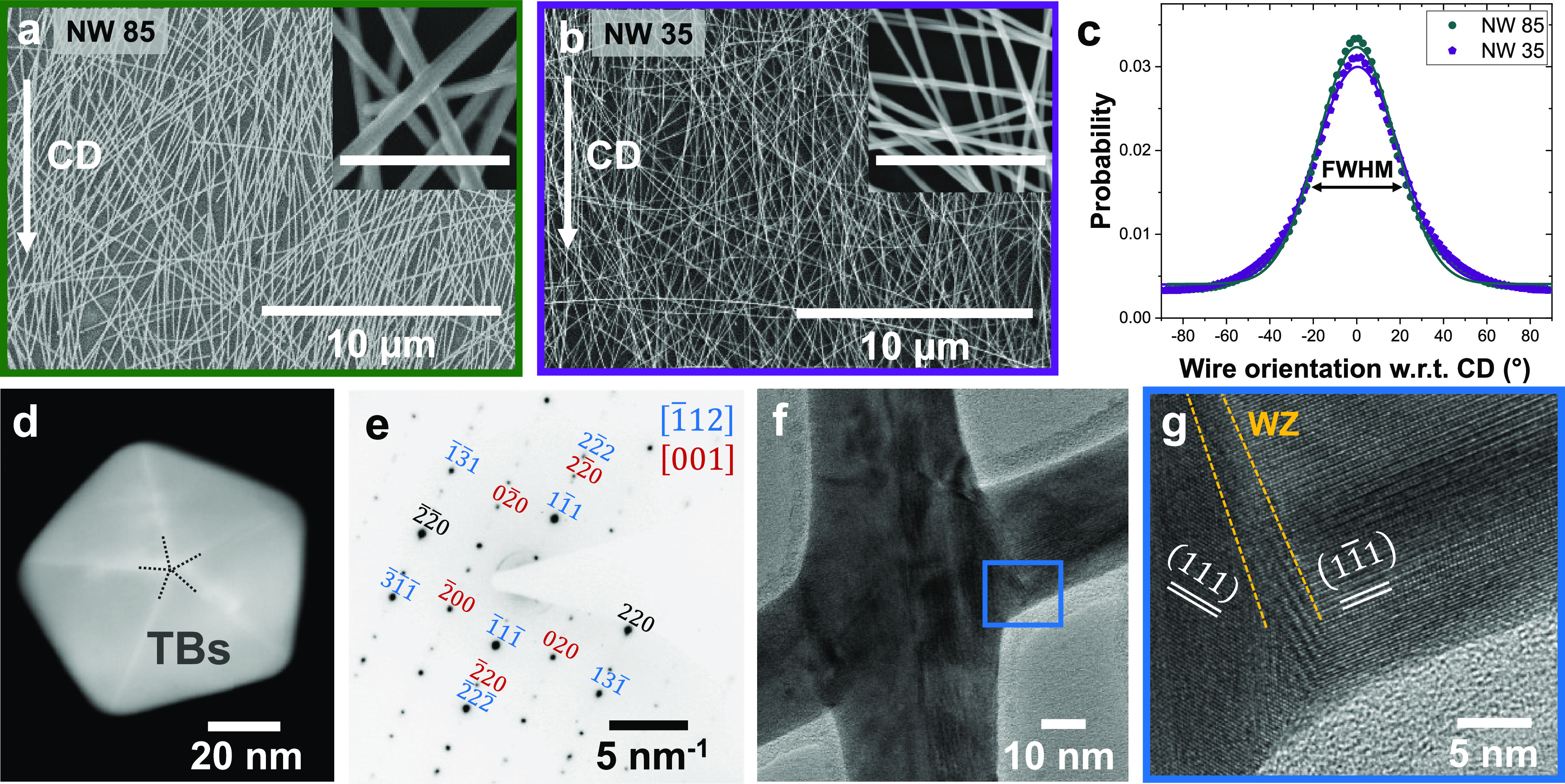
Nanowire network characteristics. (a and b) Doctor-bladed AgNW networks. The coating direction (CD) is indicated by white arrows. The average NW diameter in panel a is d̅ = 85 nm and in panel b is 35 nm. The difference in NW diameter is clearly revealed in the close-ups, where the scale bar is 1 μm. The corresponding NW networks are denoted as NW35 and NW85. (c) Probability density distribution of NW orientation with respect to the CD revealing a strongly preferred orientation in the CD (∼0°). (d) Cross-section of a AgNW depicting five twin boundaries and a pentagonal shape. (e) Selected area electron diffraction (SAED) pattern of a single NW showing superposition of two zone axes (ZAs). Common diffraction spots are black. (f) TEM image of a NW junction welded by thermal annealing. (g) HRTEM image of the junction shown in panel e illustrating the welded zone (WZ) between the NWs.
Regarding the physical properties of the AgNW networks, measurements of the sheet resistance Rs resulted in an average value of 10 ± 3 Ω/sq at an area coverage of 44% for NW35 networks and 21 ± 3 Ω/sq at an area coverage of 41% for NW85 networks, respectively. This can be understood from the fact that, for similar area coverage and NW length, the percolation of a NW network increases with decreasing NW diameter, which, as a consequence, also leads to a lower sheet resistance. With these coating parameters the optical transmittance of NW35 networks is better than 70% in the wavelength range above 450 nm, as shown in a previous study.42 The use of thinner NWs is superior to larger NW diameters regarding the electrical performance of NW networks with predefined optical transmittance.5,43 For this reason, we focused on the NW35 in the electrical measurements.
A characteristic feature of the AgNWs in both dispersions is their five-fold twinned structure, which is a result of the wet chemical synthesis, where the seed particles already contain five twins.44 Due to the lack of a chemical synthesis route of single-crystalline AgNWs for large-scale industrial applications, five-fold twinned AgNWs are the preferred choice for TCEs. The pentagonal shape with the five TBs is revealed in Figure 1d showing a scanning transmission electron microscopy (STEM) image of a NW cross-section of a NW85. The five twin segments are joined along a common quintuple line which corresponds to the common crystallographic ⟨101⟩ direction and runs along the NW axis in the growth direction.45 The angle between two {111} planes in a cubic system is 70.53°. Thus, by joining five wedge shaped twin segments, a positive partial wedge disclination of 7.35° occurs in the AgNWs associated with an inherent strain field.45 Because of the five-fold twinned structure, the diffraction pattern (DP) in plan-view geometry is typically a superposition of two pairs of crystallographic zone axes (ZAs). In the DP in Figure 1e, one twin segment is oriented along the [001] ZA, whereas two other segments are oriented along the [1̅12] ZA (see Figure S1 for a detailed DP analysis). Additional weak diffraction spots result from double diffraction. Thermal annealing of the NW networks at 100 °C was conducted in order to reduce the resistance of the individual NW junctions, thus improving the overall conductivity of the network. Upon annealing, the insulating PVP (polyvinylpyrrolidone) layer, which has a thickness of 1.3 ± 0.4 nm for the NW35 (see Figure S1) is removed and the NWs are welded together at their contact points. The HRTEM images of a welded zone (WZ) in Figure 1f,g reveal a continuous transition between the crystal lattices of the two NWs. This is in line with our earlier study where we could show that thermal annealing evokes local sintering of NW junctions by surface diffusion and homoepitaxial regrowth.46 The HRTEM images also reveal an amorphous layer around the NWs, which is even thicker than the initial PVP layer. This layer is assumed to consist mainly of PEDOT:PSS (poly(3,4-ethylenedioxythiophene)-poly(styrenesulfonate)), which was used as a sacrificial layer for the transfer of the NW network onto the TEM grid.
Combined Mechanical and Electrical Testing
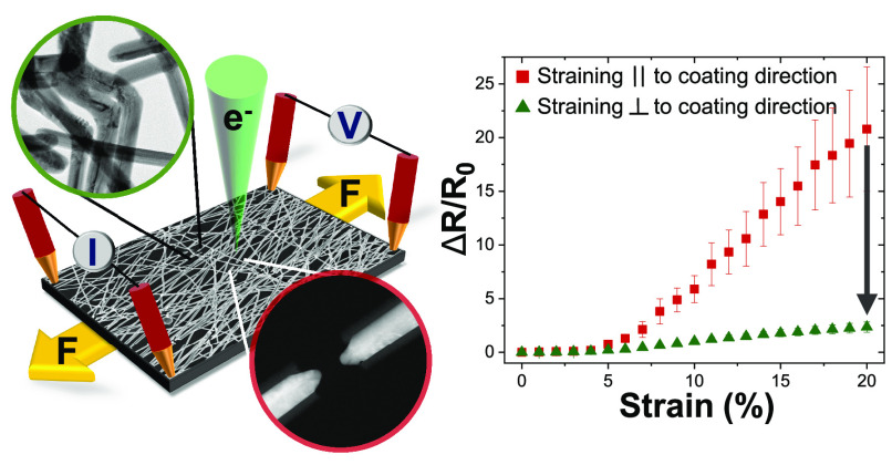
The anisotropic networks were tested by interrupted large-scale SEM tensile tests. The custom-built straining stage is designed in such a way that parallel to the straining tests electrical measurements can be performed, as illustrated in the schematic in Figure 2a. In order to investigate the effect of network anisotropy on the electrical and mechanical performance, two batches were tested. The first batch was strained parallel to the CD, and the second one was strained perpendicular to the CD. Figure 2b shows the relative increase in resistance in straining direction (ΔR/R0) as a function of engineering tensile strain revealing a pronounced difference between the two batches. For 20% tensile strain (elongation), the batch strained parallel to the CD shows a relative resistance increase of ΔR/R0 ≈ 21. In contrast, the resistance increase of the second batch, which was strained perpendicular to the CD, is almost one order of magnitude lower, ΔR/R0 ≈ 2.4. This effect can be attributed to the different microscopic deformation mechanisms, as will be discussed in the following. Moreover, it reveals that the impact of network anisotropy and influence of the NW orientation with respect to the applied load are in line with previous studies on prestraining, where biaxially prestrained samples could exceed the ones with uniaxial prestrain with respect to the electrical response during straining.47,48
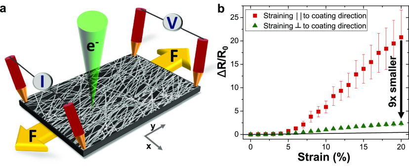
Correlated electrical and mechanical testing. (a) Schematic illustration of the experimental setup for resistance measurements during straining (in y-direction) and combined investigations by electron microscopy. (b) Relative resistance change in straining direction versus engineering strain during tensile tests for two batches of NW35 networks, where the straining direction is parallel (red) or perpendicular (green) to the CD, respectively. The black line indicates the resistance change due to the elongation.
When the straining direction is parallel to the CD, i.e. most of the wires are aligned in straining direction, single NWs fracture in tensile mode when the strain reaches ∼3% (Figure 3a). Because of the small number of fracture events, still no measurable increase in the resistance of the NW network is observed at this strain level (Figure 2b). It is noteworthy that tensile fracture does not directly occur at the NW junctions, but often occurs close to them because of strain concentrations. This indicates that the NWs are strongly welded together so that the junctions can withstand the acting stresses without detachment. In other words, the junctions are not the weakest points of the network under tensile stress. Consequently, cracks are often deflected along horizontal NWs, as it is shown in Figure 3a and schematically in Figure 3b. At 5% strain, more NWs start to fracture, which is then also visible in the electrical measurements, as the percolation of the network decreases. With increasing strain, the number of fractured NWs increases, which results in horizontal cracks in the network, extending over up to tens of micrometers, as exemplarily shown in Figure 3c,d. This shows that rupture of NWs occurs in a spatially correlated way indicating that stress transfer from one rupturing NW to neighboring NWs (via the substrate or via NW junctions) takes place. This is similar to stress transfer in fiber-reinforced composites.49,50 Moreover, the occurrence of periodic cracks in the NW networks is reminiscent of crack patterns in thin films that are strained in tension.41,51 NWs in sparse networks also develop periodic cracks upon tensile straining, as will be shown below. In comparison to dense networks, the crack spacing is larger and cracks in different NWs are spatially uncorrelated (see Figure 5c,i).
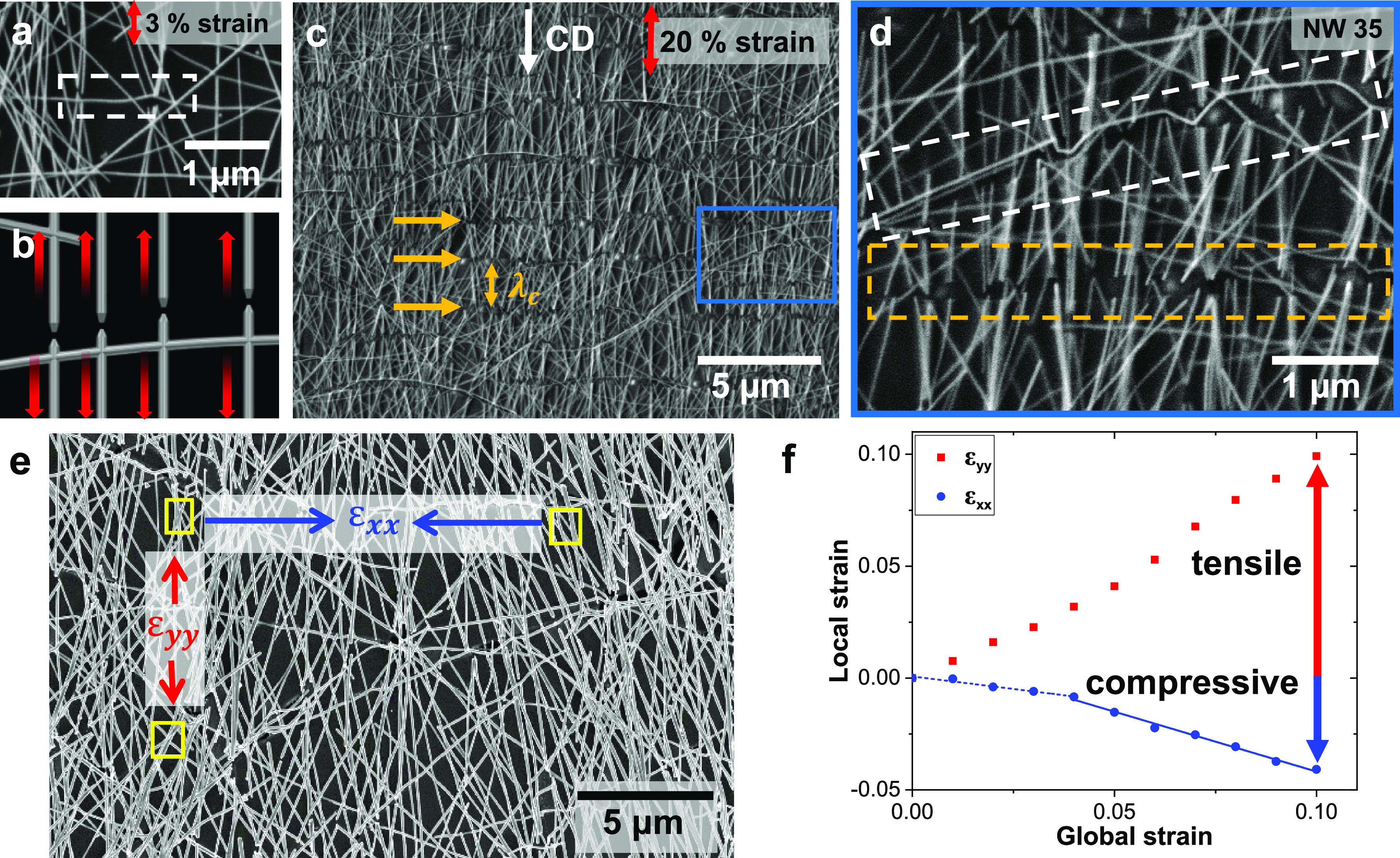
Deformation of NW networks strained parallel to the CD. (a) Close-up of fractured NWs at 3% strain (NW35). (b) Schematic of crack deflection along horizontal NWs. (c) SEM image of a NW35 network strained to 20%. Extended cracks in the network are exemplarily highlighted with yellow arrows. The average crack spacing is denoted as λc. The SEM images were taken under load. (d) Close-up of an area in panel c illustrating correlated and extended cracks of NWs. (e) Uniaxial strain (in y-direction) causes a compressive strain in transverse direction (x-direction). The local strain is determined from an SEM image series of NW85 (see SI Movie 1).The yellow rectangles mark the areas which were used for feature tracking. The image shown was taken at 10% global strain under load. (f) Local tensile and compressive strains, εxx and εyy, as determined from the image series, versus the global (applied) tensile engineering strain. The dashed and continuous blue lines indicate a change in Poisson’s ratio of the PET foil due to transition from elastic to plastic regime.
The uniaxial strain causes a contraction in the transverse direction. In the elastic regime the ratio of the axial and the transverse strain is defined as Poisson’s ratio. The NWs show a strong adhesion to the PET substrate, as no delamination or out-of-plane buckling is observed. The good adhesion is assumed to be promoted by polymer binder in the NW dispersion as well as residual surfactant PVP. Indeed, an organic intermediate layer with a thickness in the range of 1–10 nm at the substrate–NW interface can be clearly identified from cross-sectional EELS and EDX measurements (see Figure S2). All the microscopic observations support the conclusion that the PET foil effectively transfers the strain to which it is subjected to the adhered NWs. PET has a Poisson’s ratio of 0.37–0.44 for elastic deformation and shows plastic yielding at ∼ 3.5% strain.52 To confirm the compressive strain in transverse direction, the local strain in x- and y-directions was evaluated using automated feature tracking (see Figures 2a and 3e,f). At a global tensile strain of 10% in the y-direction (read from the straining device), a local strain value εyy of 9.9% was determined. This indicates that the applied tensile strain is evenly distributed across the sample. The corresponding transverse compressive strain εxx was determined as 4.1% using feature tracking. As expected,41,53 at the transition from elastic to plastic deformation, a change of the contraction ratio (i.e., “plastic Poisson’s ratio”54,55) to 0.5 in the plastic regime was observed (Figure 3f).
The second batch of samples was strained perpendicular to the CD. The observed deformation mechanisms differ strongly from the first batch. The most obvious difference is that no long-range cracks occur. As shown in Figure 3e,f, the PET foil is under compressive strain in the transverse direction. Because most of the NWs are aligned perpendicular to the straining direction, the NWs are subjected to compressive stress rather than tensile stress. As a consequence, triangular kinks (or in-plane buckles) and boat-like structures form, depending on the local network structure (yellow and green highlights in Figure 4a and schematics in Figure 4b,c). This is also observed in the first batch, which was strained parallel to the CD, for those rare NWs oriented perpendicular to the straining direction, as can be seen from Figure 3d. In cases where several parallel NWs are compressed (see Figure 4a,e), the deformed NWs are reminiscent of kink bands, which form in layered crystals when compressed parallel to their layers.56−58 Because the dominating deformation mechanisms differ from the first batch, the electrical performance of the TCEs highly differs, too. The relative resistance increase is significantly smaller, when the sample is strained perpendicular to the CD, because the percolation of the network is maintained up to high strain levels. This is clearly visible in the overview SEM image in Figure 4d. Even though a slight resistance increase of ΔR/R0 = 0.2 ± 0.07 is already observed at 5% strain, the change of ΔR/R0 at 20% strain is only 2.4 ± 0.5, which is almost one order of magnitude lower compared to samples strained to the same extent in the CD. Keeping in mind that the initial sheet resistance is 10 Ω/sq, the TCE sustains a high conductivity at 20% strain. The resistance increase based purely on geometric considerations can be calculated as ΔR/R0 = 2ε + ε2.59 At 20% strain this corresponds to a relative resistance increase of 0.44. Moreover, because of the compressive stress in the transverse direction, the resistance in this direction slightly decreases during straining, and the evolution of both batches is comparable (see Figure S3).
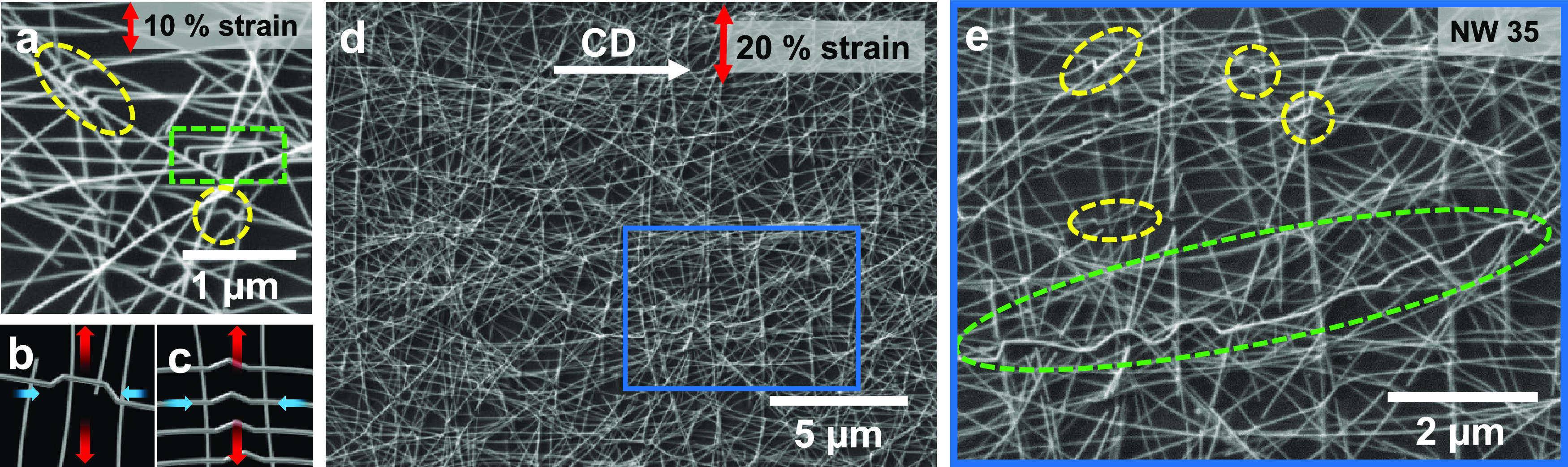
Deformation of NW35 networks strained perpendicular to the CD. (a) Close-up of kinked NWs at 10% tensile strain. Boat-like structures (green highlight) and triangular kinks (yellow) are observed. (b and c) Schematic kink formation due to transverse compressive stress. (d) SEM image of a NW network strained to 20% perpendicular to the CD illustrating the high degree of percolation at this strain level (image taken under load). (d) Close-up of an area in panel c showing kink formation and local fracture.
The results presented in Figures 2–4 show that the electrical performance of a NW network is closely connected to its mechanical deformation behavior. In general, the deformation can be categorized into three basic deformation modes. Mode A is tensile fracture of NWs, which is the dominant mode, when the network is stretched parallel to the CD. Mode B is kink formation of NWs due to compressive strain. This is the dominant mode observed for stretching perpendicular to the CD. In contrast to the first two modes, which also occur for single NWs (see below), the third mode occurs only in dense NW networks and can be described as nanowire bending, similar to the conditions in a three-point bending test (see Figure S4). This mode is a combination of modes A and B and is caused by the influence of surrounding and attached NWs. To gain a deeper understanding of these deformation modes and the crystal defects involved, a detailed microscopic study was performed and interpreted with the help of MD simulations.
The deformation under tensile strain (mode A) is further investigated by in situ TEM tests of single NWs and SEM tensile tests of sparse NW networks (Figure 5). When a sparse network on a PET foil is subjected to tensile strain, isolated NWs oriented parallel to the loading direction show multiple periodic fracture events as revealed in Figure 5c for a strain of 50%. The defects involved in deformation mode A were further investigated at nanometer scale by in situ TEM tensile tests of single NWs with diameters between 65 and 300 nm in displacement-controlled mode (strain rates in the range of 0.8–2 nm/sec). The wires were transferred on a push-to-pull (PTP) device and fixed on both ends with carbon patches deposited in a focused ion beam (FIB) instrument (Figure 5a). All tested NWs first show nucleation of defects distributed along the gauge length, followed by highly localized deformation and necking at one region.60 Subsequently, the NWs fracture at this location (Figure 5e–h). The fractured ends are tapered, which is indicative of ductile fracture. In situ (S)TEM imaging directly reveals the formation of stacking faults (SF) on slip planes inclined to the NW axis (Figure 5e–h and SI Movie 2). In the micrographs extracted from the in situ videos the SFs appear as straight line contrast (see Figure 5e–h). In order to provide evidence of the nucleation of SFs upon straining, individual SFs are highlighted in the two STEM images of Figure 5g. As the NW was strained further, a new SF was formed, highlighted in yellow. Moreover, due to the five-fold twinned structure slip systems in different twin segments are activated (see Figure S5). The angle between two SFs is measured as ∼70° which corresponds to the angle between different {111} slip planes. SFs are formed by nucleation and glide of Shockley partial dislocations which then interact with the TBs of the NW. The role of the TBs and details of dislocation reactions are further investigated by MD simulation (see below). However, already from the experimental images it is evident that under tension no deformation twinning as in the case of single crystalline fcc wires occurs.61 From the engineering stress–strain curve in Figure 5b, the yield strength of the NW with a diameter of 215 nm is estimated to be 740 MPa, applying the 0.2% strain criterion. The engineering yield strain is about 1.5%. The serrated curve indicates sudden dislocation bursts, which are likely associated with the TBs acting as barriers for dislocations and thus require higher stresses for dislocation transmission or nucleation of new dislocations. After the onset of yielding, the stress slightly increases, further indicating moderate strain hardening, which can be attributed to the presence of TBs and stored defects.62−64 The ultimate tensile strength is 820 MPa at a strain of 3%, which is in good agreement with previous results reported in the literature.62,63 Pronounced necking occurs in a highly localized region (Figure 5h), where a small wire segment is then locally strained up to double its initial length. The corresponding NW fractured at an engineering strain of about 7%. Compared to polycrystalline bulk silver with a coarse-grained microstructure with a yield strength of 55 MPa,65 the five-fold twinned NWs show a more than one order of magnitude increased yield strength. This size effect of strength in the submicrometer range is well-known and reported in the literature for thin films, pillars, wires, and whiskers.66,67 The effect is explained by dislocation starvation, dislocation source truncation, and exhaustion hardening.66 In twinned NWs the size effect is determined not only by the NW diameter, but also by the TB spacing. This is supported in the literature by tensile tests of AgNWs with TBs along the ⟨112⟩ wire axis that suggested that the size effect of strength is dominated by the size of the largest twin segment.68 Regarding the elastic properties of the NW, a Young’s modulus of ∼70 GPa can be estimated from the in situ TEM experiment using the initial slope of the stress–strain curve. This is slightly smaller than the bulk modulus of Ag in the [101] direction (83.8 GPa)60, but comparable with values extracted from other in situ studies of AgNWs.68
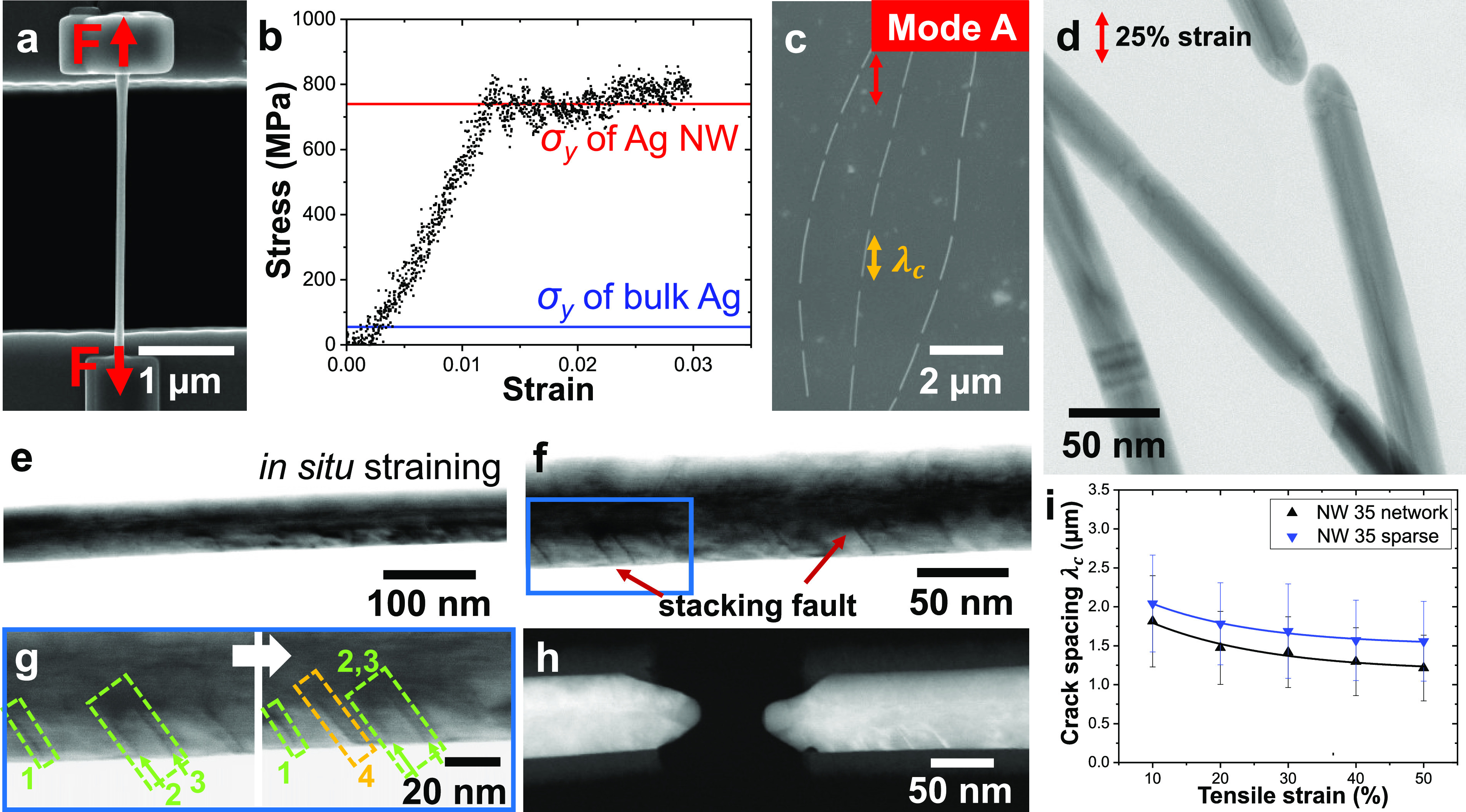
Ductile fracture of NWs under tensile stress (deformation mode A). (a) SEM image of a single AgNW glued on a PTP device for in situ tensile testing. (b) Representative engineering stress–strain curve for a wire with a diameter of 215 nm. The yield strength σy of the wire is about 14 times higher than for bulk Ag indicating a strong size effect. (c) Single NWs illustrating failure due to multiple tensile fracture. (d) Bright-field (BF) TEM image of a sparse network strained up to 25% elongation illustrating the local deformation with necking and ductile fracture. (e–h) STEM images of an in situ tensile test of a AgNW (d = 65 nm). Stacking faults that formed by partial dislocations on {111} planes are indicated by red arrows. (g) Two close-ups of the area marked with a blue frame in panel f. A new stacking fault is highlighted in yellow. (h) The fractured NW ends are tapered because of localized necking. (i) Average crack spacing of dense and sparse NW35 networks as a function of tensile strain.
Localized deformation and necking of NWs is observed in the network, too, as it is clearly seen in the BF TEM image in Figure 5d. Additionally, the crack spacing as a function of the global tensile strain has been compared for sparse networks (Figure 5c) and dense networks (Figure 3c). In both cases, the average crack spacing (λc) shows a significant decay with a saturation around 50% tensile strain (Figure 5i). This evolution of crack spacing is also observed for thin films under tensile straining.41,51 In the dense NW network, λc amounts to 1.8 ± 0.6 μm for 10% tensile strain, and it decreases to 1.2 ± 0.4 μm for 50% strain (Figure 5i). The crack spacing of sparse NW networks is always slightly larger. This can be attributed to the increased mutual interaction of NWs in a dense network supporting local stress concentration, crack deflection, and correlated rupture.
The second deformation mode (mode B) that was identified in the straining experiments on NW networks is kink formation, which results from compressive stresses induced by the transverse contraction of the PET substrate during uniaxial straining (Figure 3e,f).41,48,51 This mode can be observed in pure form in single NWs oriented perpendicular to the straining direction, which experience compressive stress without being affected by adjacent NWs or NW junctions (Figure 6). Regarding the NWs deformed in compression, a key finding is the formation of periodic triangular kinks, which results in a serrated NW structure (Figure 6a). This is in contrast to previous studies of Ag-coated PVB-nanofibers, Si NWs, and carbon nanotubes on prestrained polydimethylsiloxane (PDMS), where sinusoidal buckling was observed under compressive stress.48,69−71 In the elastic regime the buckling is assumed to be controlled by the NW radius and the Young’s moduli of the NW and the substrate.70 Because PET is a thermoplastic and PDMS an elastomer, the Young’s moduli differ by more than 3 orders of magnitude with PDMS being much more compliant. This might be part of the reason for the different behavior. As discussed above, the NWs show a strong adhesion to the PET, which is also assumed to promote local strain concentrations and therefore kink formation. However, with respect to devices, strong coupling of NWs to the substrate is often highly desirable to prevent delamination, out-of-plane buckling, and possible short circuits. Moreover, the kink formation of the AgNWs observed in the present work is largely controlled by plastic deformation involving formation of crystal defects. For plastic deformation, the five-fold twinned structure of the NWs plays a key role favoring local kinking by GB formation, as discussed in more detail below. It is noteworthy that the NWs show an extremely high plastic deformability under compression. In contrast, single crystalline fcc NWs are expected to show shear failure under compression by dislocation slip.60,72 Upon extended straining, the NWs form kinks with increasing acute angles without failing by fracture (Figure 6a,b). A high deformability of five-fold twinned AgNWs under compression was also observed by Vlassov et al.73 during in situ SEM bending tests. However, beside kink formation these authors also observed crack initiation at the point of the highest curvature. For our sparse networks we quantified the evolution of kink geometry as a function of strain by evaluating the kink angle (αK) and kink distance (dK), as illustrated in Figure 6b and plotted in Figure 6c. The average kink angle decreases from 116 ± 17° at 10% strain to 70 ± 39° at 50% strain, while the kink distance decreases from 2.5 μm at 10% strain to 1.0 μm at 50% strain. Interestingly, even in the case of local fracture no gaps between fractured ends occur. Rather, sliding of the fractured ends in combination with cold-welding takes place. This is clearly visible from the HAADF image in Figure 6d, which furthermore shows that the NW cross section is largely retained in the welded zones. This finding is of key importance in view of the application of such NW networks as flexible electrodes, because the cold-welded kinks are assumed to still be electrically conductive.
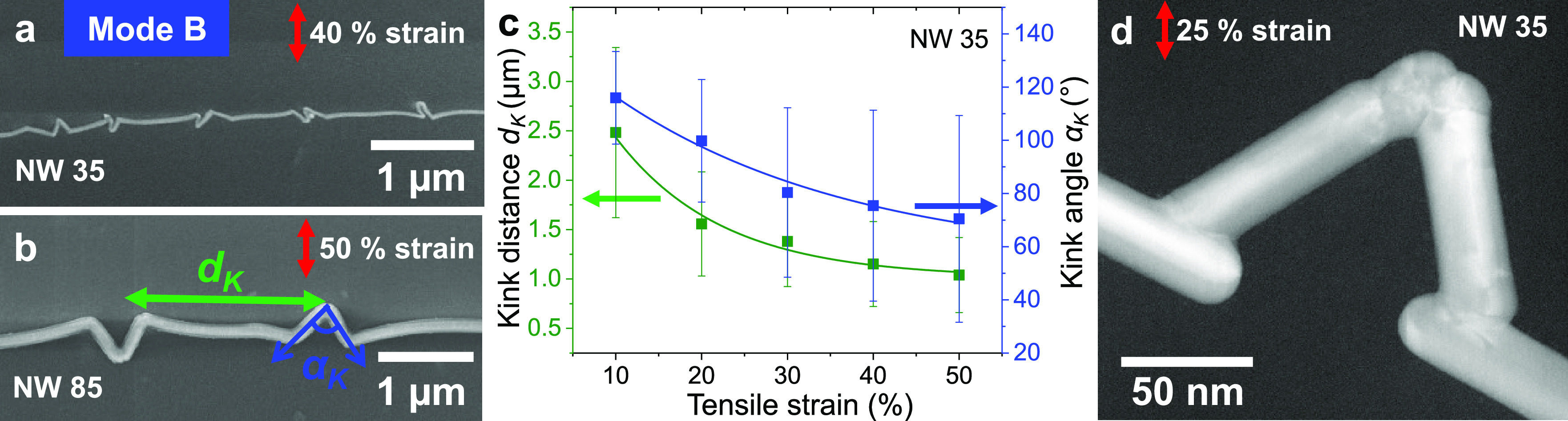
Kink formation in NWs under compression (deformation mode B). (a) Single NW after 40% tensile straining of the PET foil perpendicular to the wire orientation illustrating the formation of periodic triangular kinks. (b) The NW kink geometry is defined by the kink angle αK and the kink distance dK. (c) Evolution of the mean kink angle and distance as a function of tensile strain. (d) High-angle annular dark-field (HAADF) STEM image of a triangular kink at 25% strain showing cold-welding after fracture. The micrographs were taken after unloading of the samples.
HRTEM Studies of Kink Formation and Related Defect Structures
Here, we focus further on the analysis of defects involved in the formation of triangular kinks by means of TEM and MD simulation. The TEM image in Figure 7a shows part of a AgNW network, which was originally coated on a PET substrate and strained ex situ to 25% tensile strain perpendicular to the CD. After straining, the network was released from the PET substrate for plan-view TEM investigation. From the TEM micrograph it can be seen that several NWs aligned parallel to the straining direction fractured in tension. The NWs oriented perpendicular to the aforementioned deformed by kinking. In the following, we focus on the area marked by a blue frame, where two parallel NWs formed correlated kinks with identical kink angles of αk ≈ 135°. The HRTEM image of this area (Figure 7b) shows that the kinks are composed of sharp GBs, where most of the defects accumulate. In the top NW, two grain boundaries (GB1, GB2) are present in the kinked region to accommodate for the deformation, whereas the thinner NW below shows only one grain boundary (GB3). The difference is probably caused by the constraint the lower NW puts on the deformation of the top NW, enforcing a larger radius of curvature in the kinked region. Moreover, the top NW is thicker compared to the lower one, further supporting a larger radius of curvature. In order to determine the nature of the grain boundary GB1, local fast Fourier transformation (FFT) is employed. The FFTs at each side of the GB (Figure 7c) are identical, but they are rotated by 20.5° relative to each other (the FFTs show the same NW orientation as the DP in Figure 1e). This means that GB1 is a pure tilt grain boundary in this segment of the five-fold twinned NW. The enlarged HRTEM image of grain boundary GB1 in Figure 7c reveals a periodic dislocation contrast along the GB. These dislocations likely nucleated at the top surface of the NW as a result of tensile stress due to bending and aligned on top of each other, thus forming the tilt GB. The average distance between two dislocations is measured as dD = 0.83 nm. If the dislocations possess a Burgers vector b, the distance d between dislocations is related to the tilt angle of the GB via Frank’s rule: .74 Assuming full dislocations with Burgers vector a/2⟨110⟩, the calculated tilt angle is 20°, which is in almost perfect agreement with the tilt angle (20.5°) directly measured from the HRTEM image by evaluating the relative rotation of the crystal lattices across the GB. Moreover, GB2 has the same orientation as GB1 and a tilt angle of 24° (see Figure S1).
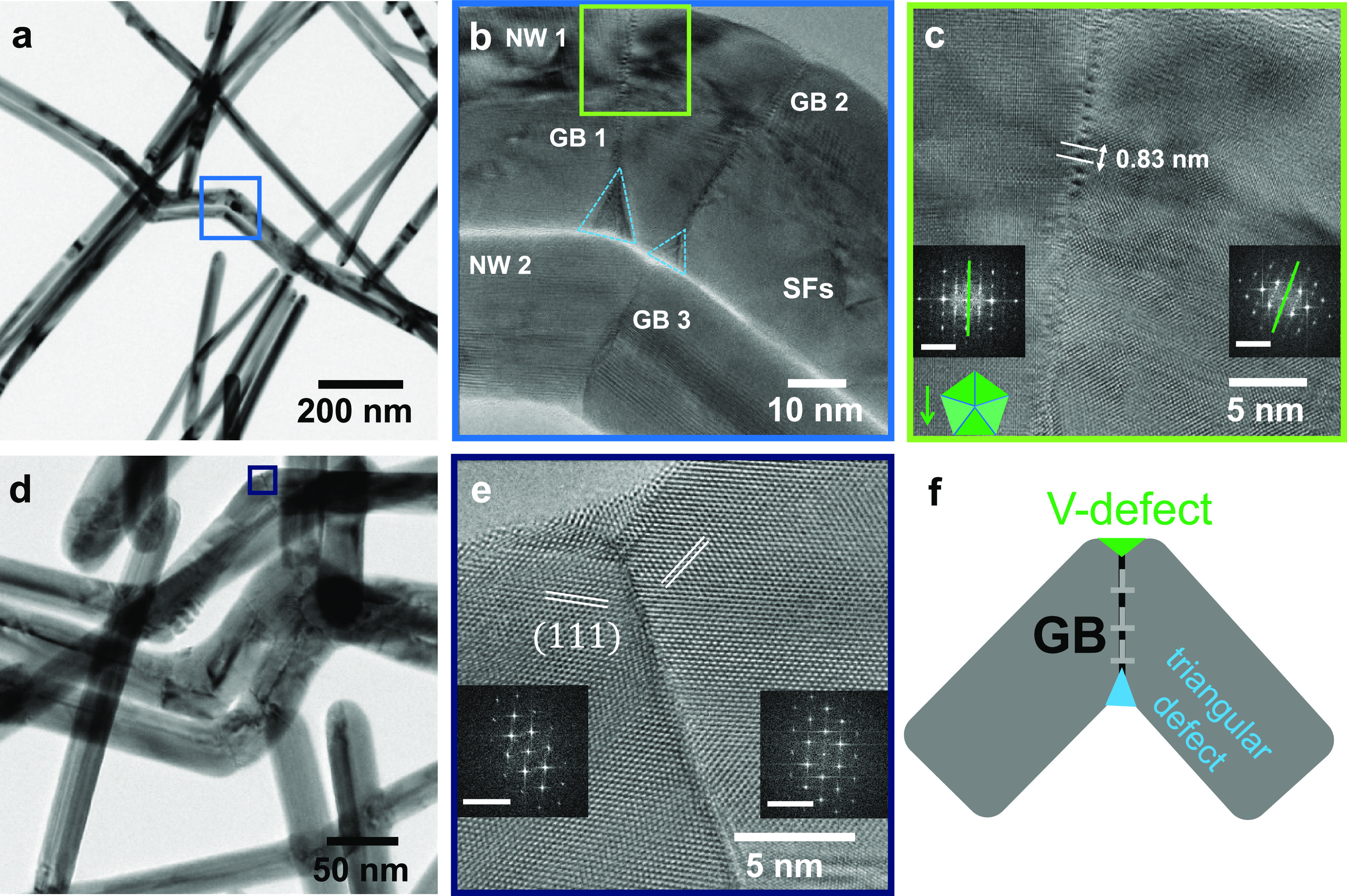
HRTEM analysis of triangular kinks. (a) TEM BF image of a AgNW network strained perpendicular to the CD (25% tensile strain, unloaded) revealing characteristic kink formation. (b) Close-up of the kinked wires in panel a illustrating GB formation. Triangular defects at the end of the formed GB are marked with blue dashed lines. (c) HRTEM image of the wire in panel b marked with a green square depicting single dislocations at the grain boundary. The insets show the FFTs of the wire on the left and right side of the GB. The scale bar is 10 nm–1. The schematic NW cross-section illustrates the orientation with respect to the electron beam (green arrow). (d) BF TEM image of a kink with a V-defect at the NW top. (e) Close-up of the V-defect in panel d. The GB dissociates along two inclined {111} planes similar to the case of “chevron defects” reported in the literature.75 The scale bars in the FFTs correspond to 10 nm–1. (f) Schematic of a kink illustrating the involved defect structures.
Another interesting observation is that both NWs in Figure 7a,b show a triangular-shaped defect at the bottom of the kink where the kink forms an acute angle. This defect occurs at the end of the formed GB. During NW bending and kink formation, tensile and compressive stresses occur above and below the neutral plane, respectively. The highest compressive stress appears in the concave region at the bottom of the NW. Obviously, defect processes are initiated which redistribute excess material into a triangular-shaped subgrain. Another significant feature of the kinked wires is a V-shaped defect at the intersection of the GB with the free surface on the convex side of the kink (cf. schematic in Figure 7f). The V-defect occurs in the part of the NW that is under tensile stress (e.g., Figure 7d, area marked by blue frame). From the HRTEM image in Figure 7e, the GB is again identified as a pure tilt grain boundary with a tilt angle of 50°, as can be deduced from the two FFTs taken on either side of the boundary (see Figure S1). Similar V-defects were observed by HRTEM in gold at the intersection of a 90° ⟨110⟩ tilt GB with a free surface.75,76 Such “chevron defects” have been interpreted as energetically favorable surface reconstructions of the GB. In the same way, the GB in the AgNWs dissociates near the surface, and the boundary splits into two inclined boundaries parallel to the (111) planes, as clearly revealed in Figure 7e. The height of the V-defect is about 2 nm. Because V-defects involve stacking faults (see also atomistic simulation, Figure 8), the driving force for the formation of these defects is expected to be closely related to the stacking fault energy (γsf). In fact, the chevron-defect mentioned above has been observed in Au (γsf = 32 mJ/m2), but not in Al, which shows a more than four times larger stacking fault energy (146 mJ/m2). Ag has an even lower stacking fault energy (16 mJ/m2)77 than Au, which is expected to further support the formation of V-defects. This explains the energetic stability of formed V-defects. Moreover, in a previous MD study78 on [110] single crystalline Au NWs formation of a similar defect structure, a wedge-shaped twin was observed in the tensile strained part of the NWs under bending. We think that V-defects play an important role in the excellent mechanical deformability and electrical integrity of AgNWs under compressive and bending stresses.
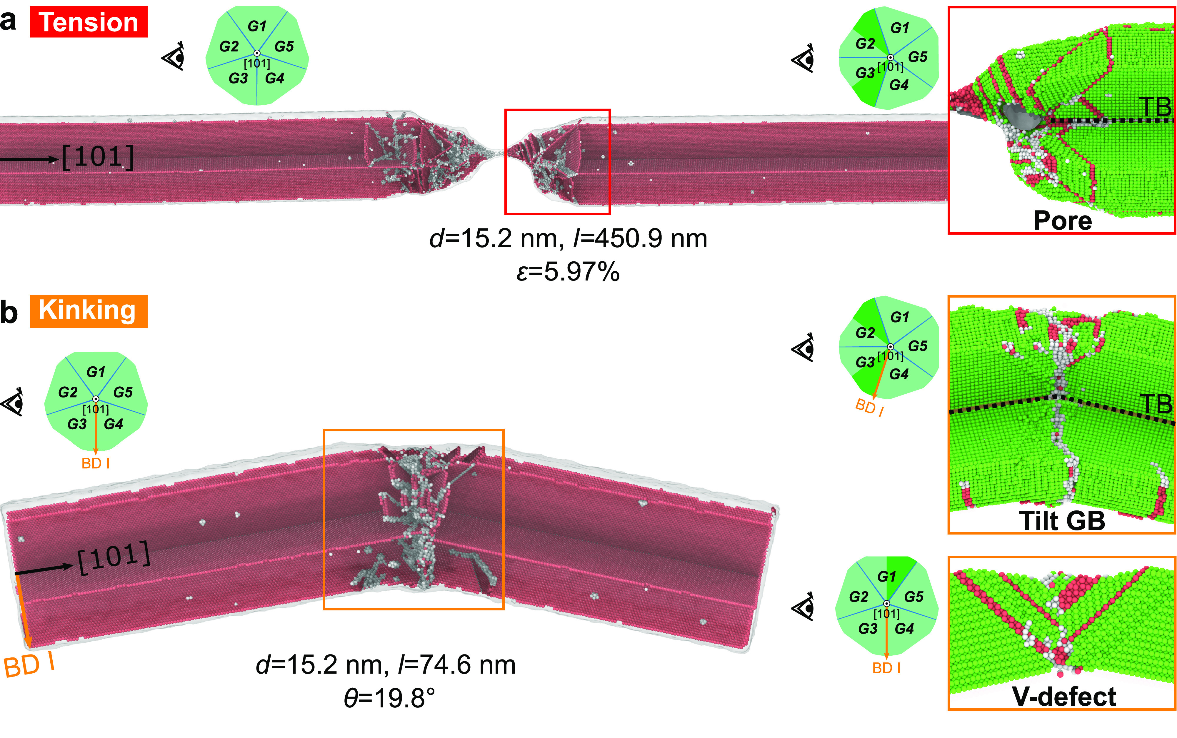
MD simulation results of five-fold twinned AgNWs under different loading conditions. (a) Fractured AgNW under tension at 5.97% strain. Only atoms belonging to TBs and defects are shown here. Surface mesh is half-transparent. The inset shows the pore formation at the zoomed-in fractured end. The NW is sliced and visualized according to the schematic in the inset to illustrate internal defects; only dark green parts are visible. The outer-layer atoms are removed. Atoms are colored according to the common neighbor analysis. Green, red, and white atoms indicate fcc, hcp, and unidentified structural types, respectively. (b) Deformed configuration with bending angle θ = 19.8° after bending test along bending direction (BD) I and 400 ps relaxation after load removal. The inset shows the formation of tilt GB and V-defect. The GB penetrates from G3 to G2 and dissociates at the V-defect in G1 along two conjugated {111} planes. The V-defect consists of a wedge-shaped twin and stacking faults.
To compare with literature, Hwang et al.79 performed cyclic bending fatigue tests on five-fold twinned AgNWs and observed the formation of subgrain boundaries in wavy buckles. They proposed that the subgrains form because of geometrically necessary dislocations (GNDs), but they could not resolve the dislocations by TEM. Furthermore, Wang et al.80,81 used multiply twinned ⟨112⟩-Ni NWs for studying the mechanically induced GB formation under bending. They observed the formation of low-angle GBs, which consist of randomly distributed dislocations in a diffuse GB layer. Further bending evoked lattice distortion, followed by dynamic recovery and formation of high-angle GBs. In our study on AgNWs, the formed high-angle GBs show a narrow GB zone, where the dislocations arrange in a wall, as revealed in Figure 7c. Recently, Zhao et al.82 studied the geometrical constraints in five-fold twinned AgNW kinks, which formed in bending tests. Using scanning nanobeam electron diffraction, they analyzed the orientation of the GBs and found, consistent with our results, that pure tilt GBs form.
Atomistic Simulations of Nanowire Deformation and Failure
To further understand the deformation mechanisms of AgNWs on the atomic scale, we performed MD simulations on individual NWs with diameter of 15.2 nm put under tensile and bending strain (see Figure S6 for the MD simulation setup). In the case of the simulated tensile test, the plastic deformation is carried mainly by nucleation of leading partial dislocations at the free surface and multiplication of these dislocations at the TBs. Under tension, the Schmid factor of the leading partial dislocation on the primary slip systems in ⟨110⟩-oriented NWs is two times higher than that of the trailing partial dislocation; therefore, the nucleation of leading partial dislocations is more favorable.61,72 Plasticity is initiated at a strain of 3.56% (see Figure S7b). The TBs strengthen the AgNW by impeding the propagation of partial dislocations (see Figure S7). This explains the observed accumulation of stacking faults in the in situ TEM tests and the strain-hardening noticed in the stress–strain curve (see Figure 5). Moreover, a pore forms close to the quintuple line in the region where fracture occurs. As already revealed in our earlier MD study,60 this pore formation can be attributed to the evolution of positive hydrostatic pressure (tension) in the wire center upon tensile loading. The stress field associated with the central wedge disinclination is in the unloaded state negative (compression) in the axial and radial directions, but due to the elastic anisotropy of silver changes to tensile upon loading. As a result, defect processes are initiated which result in the pore formation.60 In contrast to deformation twinning-mediated plasticity in ⟨110⟩-oriented single-crystalline NWs under tensile strain,61,72 five-fold twinned AgNWs show strongly localized plastic deformation, as illustrated in Figure 8a. The plastic localization phenomena in the AgNWs can be attributed to the five-fold symmetry of the crystallographic arrangement. The pre-existing TBs truncate slip planes, resulting in an enclosed five-fold symmetric slip system, as illustrated in Figure S6b; thus, the possibilities for dislocation glide along the primary slip planes are restricted in a confined region. The deformation process of the simulated AgNW under tension is shown in SI Movie 3.
In the case of the simulated bending test, plasticity is initiated by nucleation of partial dislocations from the tensile part, followed by nucleation of full dislocations from the compressive part (see SI Movie 4). This transition of deformation mechanism upon changing the loading condition can be explained by the interchange in Schmid factor between leading and trailing partial dislocations.72 In the compressive part of the NW, dislocations on the different slip planes interact with each other by forming dislocation locks containing sessile dislocations.77 The interlocked dislocation networks act as a barrier to the glide of further dislocations, and these dislocations accumulate in the incipient GB region. The accumulation of further dislocations at the GB region results at a bending angle of 19.8° in a tilt GB (see Figures 8b and S8) in agreement with our HRTEM observations (Figure 7c). Moreover, the formation of a V-defect at the top of the NW was also observed in the MD simulations (Figures 8b and S8). Both flanks of the V-defect are composed of micro twins, which are created by partial dislocations under tensile strain on two conjugated slip systems. A similar mechanism was revealed in our previous MD simulations of bending tests on ⟨110⟩-oriented Cu and Au single-crystalline NWs.78 In contrast to the single-crystalline NWs, which show pseudoelasticity after load removal,78 kink formation hinders the unbending process of the five-fold twinned AgNW (see SI Movie 4), which implies a better reversibility upon bend deformation of single-crystalline NWs. The bent AgNWs in BD II and III (see Figure S8) show resulting defects similar to the wire bent in BD I. In addition, the triangular-shaped defect in the compressive part of bent NWs, which was identified by HRTEM (see Figure 7b), was also observed in the simulated NWs with large bending angle (θ > 30°) (see Figure S8).
Impact of Network Anisotropy on Mechanical and Electrical Failure
On the basis of our experimental observations and atomistic simulations, we propose a simplified model which explains the strong impact of network anisotropy on the deformation and failure of highly textured AgNW network electrodes (Figure 9). Depending on the NW orientation with respect to the applied load, deformation under tensile strain, kink formation in compression, or bending takes place. Because of the interconnection of NWs in a network, the deformation of a NW in the network can often be described as a combination of these three deformation modes. However, when a highly textured network is strained in the direction of the preferred wire orientation (coating direction, CD), most of the NWs fail in tensile mode. Periodic cracks in the network form, which eventually lead to a loss of percolation. As a result, a significant increase in the resistance along the straining direction is already observed at moderate strain values (Figure 2). In contrast, when the strain is applied perpendicular to the preferred wire orientation, most of the NWs deform in compression and form kinks, which sustain a percolated network. Therefore, a low resistance is retained up to high strains. This is exactly the behavior that we observed in our resistance measurements of highly textured NW networks under uniaxial straining (Figure 2). In the illustration of the model in Figure 9, only two wire orientations, parallel and perpendicular to the CD, are depicted for simplicity. After coating, most of the NWs are aligned in the CD and only a few are perpendicular (center). Straining parallel and perpendicular to the CD leads to the described behavior, as illustrated in the left and right parts of the Figure 9, respectively. In a real network, NWs also appear in inclined directions, thus experiencing a combination of tensile and compressive strain. However, this does not change the overall behavior of the NW network and is therefore neglected in the simplified sketch in Figure 9.
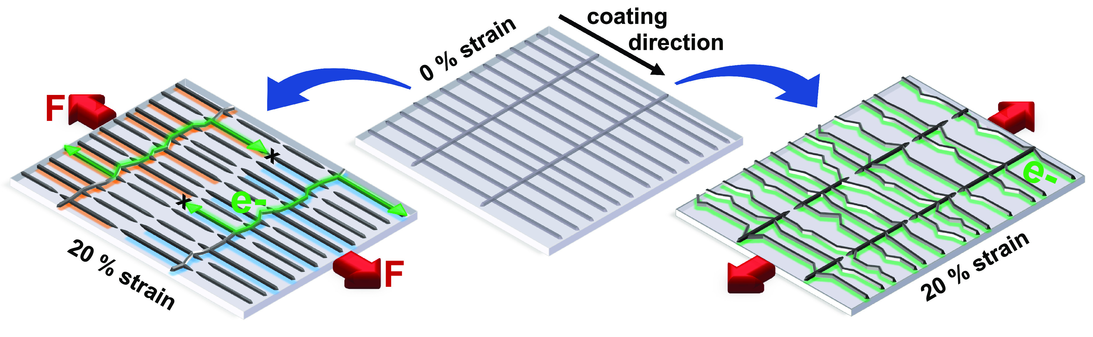
A simplified model of the deformation mechanism of a highly textured NW network. The network structure at 0% strain is depicted in the center. The coating process of the NWs causes a preferential orientation of the NWs in the CD. On the left side the network is strained parallel to the preferred wire orientation. As a result long-range periodic cracks form and deteriorate the electrical percolation of the network. On the right side the network is strained perpendicular to the preferred wire orientation. Because of the formation of kink structures, a high percolation is maintained. For simplicity, only NWs parallel and perpendicular to the CD are displayed in the model.
Conclusions
The microscopic deformation and failure modes of anisotropic networks of five-fold twinned AgNWs prepared by doctor blading on PET substrates were studied under uniaxial straining. The results were directly correlated with changes in resistance of the networks, which is the key electrical performance parameter for their use as transparent conductive electrodes. The straining tests revealed a strong impact of the network anisotropy, which manifested itself in a one order of magnitude lower increase in resistance for networks strained perpendicular to the CD compared to networks strained parallel to the CD. The reason for the pronounced influence of network anisotropy on the maintained degree of percolation could be ascribed to the anisotropic mechanical deformation behavior of NWs aligned along different directions in the network. When the straining direction is parallel to the CD and thus to the preferential NW orientation, many NWs fail by tensile fracture. Because this occurs in a correlated way, long-range cracks are formed, which strongly reduces the percolation. For the network strained perpendicular to the CD, due to the effect of transverse contraction of the PET substrate, the majority of NWs is deformed in compression. Such NWs show kink formation without complete rupture, thus leaving the electrical percolation of the network largely intact. The characteristic microscopic deformation modes were further studied by in situ TEM experiments on single NWs, straining tests on sparse NW networks, HRTEM investigations of defect structures, and complementary MD simulations. We identified three fundamental deformation modes of five-fold twinned Ag NWs, namely, fracture due to tensile straining (mode A), kink formation as result of transverse compressive strain (mode B), and bending of NWs which experience additional constraints in the NW network (mode A+B). It is noteworthy that the AgNWs show highly localized deformation under all three modes, both in the experiments and in MD simulations. The reason for this is the 5-fold twinned microstructure of the NWs, which strongly affects dislocation glide and multiplication. Under tension, the plastic deformation is mainly carried by partial dislocations causing pronounced necking, whereby the TBs strengthen the NWs by hindering dislocation glide. Under compressive strain, the nucleation and slip of full dislocations govern the plasticity and contribute to the formation of kinks. The accumulation of dislocations at the interlocked dislocation networks leads to the formation of tilt GBs in the NW kink. V-shaped defects form at the termination of the GBs with the free surface and probably promote suppression of detrimental crack initiation on the convex side of the kink, where large tensile stresses occur. Because generation of V-defects involves partial dislocations and stacking faults, the extremely low stacking fault energy of Ag is expected to support the formation of these advantageous structural features. Finally, at high compressive strains where NW fracture cannot be completely suppressed, cold welding takes place and keeps the fractured parts of NWs in intimate contact, thus retaining their contribution to electrical percolation. In summary, we identified several advantageous properties of five-fold twinned AgNW networks regarding their microscopic deformation mechanisms and defect processes as well as the role of NW network anisotropy on mechanical and electrical performance. We expect that these detailed microscopic insights contribute to further improve fabrication and design strategies for transparent NW network electrodes for flexible and stretchable devices.
Methods
AgNW Network Fabrication
All AgNW networks were doctor bladed (Zehntner GmbH) under ambient conditions in air. NW dispersions were purchased from Cambrios Film Solutions (ClearOhm Ink-NKA) and from RAS AG (ECOS X3). According to their average wire diameter, the Cambrios NWs are labeled NW35 and the ECOS NWs NW85 in this article. A PET foil (Goodfellow GmbH) with a thickness of 23 μm was used as a flexible substrate. For doctor blading, the PET foil was attached to a glass slide with PDMS as adhesive layer. The PDMS solution was mixed with a curing agent (Dow Corning, Sylgard 184) at a ratio of 10:1 and afterwards degassed in vacuum for 10 min to remove any gas bubbles. To cure the PDMS it is annealed at 95 °C for 3 h. For the fabrication of NW networks, both NW dispersions were used undiluted and coated at 40 °C. The NW35 were coated with a speed of 1 mm/s and annealed at 100 °C for 3 min. The NW85 were coated with 3 mm/s and annealed at 100 °C for 4 min. Sparse networks were fabricated by diluting the NW35 with DI water in a ratio of 1:15 and coated with the same parameters as the dense networks. For SEM investigations the sparse networks and the dense networks, which were not tested electrically, were coated with carbon after mechanical testing by evaporation of carbon threads. To perform TEM investigations the AgNWs were coated on top of a sacrificial layer of PEDOT:PSS. PEDOT:PSS (Al 4083, Heraeus) was diluted with isopropanol in a ratio of 1:1, and the wetting agent Capstone FS-31 (DuPontTM) was added in a concentration of 0.1% with respect to the PEDOT content. Doctor blading was conducted at 60 °C, and the annealing step was performed at 150 °C for 5 min. By diluting the sacrificial layer of PEDOT in water, the NW network was transferred onto a TEM lacey grid.
SEM Straining Tests Combined with Electrical Measurements
For SEM straining tests a custom-built straining stage was designed. With a fine thread (M6x1) the displacment during a straining step was applied. For the electrical measurements a van der Pauw setup was used, and four copper wires were placed in a square with a side length of 16.6 mm. The electrical measurements were performed with a Keithely Series 2400 source meter. For all measurements the sweep range was set from −0.1 to 0.1 A. For the electrical measurements parallel and perpendicular to the straining direction, six samples were measured for each direction and averaged. The error bars represent the standard deviation for these measurements. In addition, the sheet resistance was measured on glass substrates as a reference. The SEM investigations were performed with a Thermo Fisher Helios Nanolab 660 dual beam FIB/SEM system and a Phenom ProX Destop SEM. The local strain during a tensile test was determined via feature tracking. The script was written in Python 3.6, and feature tracking routines of the openCV software library were implemented. The wire orientation of the NW networks, i.e. the PDFs, was analyzed via the directionality plugin, which is based on the local gradient orientation, of the open source software ImageJ. For the evaluation of the crack spacing of the dense and sparse networks more than 300 measurements were taken, and for the evaluation of the kink angle and kink distance more than 100 measurements were taken.
In Situ TEM Tensile Tests and HRTEM Analysis
The AgNWs for in situ tensile tests of single NWs were synthesized using the polyol reduction as it is described in our previous publication by Göbelt et al.83 The straining tests were performed with a Hysitron PI 95 TEM PicoIndenter (Bruker). The NW dispersions were drop-cast onto photolithographically patterned Si wafers. Afterward, the transfer of a single NW onto a push-to-pull device was performed inside a FIB instrument. The Easy Lift manipulator was used for the transfer, and the carbon gas injection system (GIS) was used to attach the NW to the manipulator and for the fixation of the NWs on the PTP device. The gauge length was 2.5 μm, and the misalignment of the wires relative to the loading direction was less than 5°. The straining tests were conducted in displacement-controlled mode (0.8–2 nm/s). The TEM studies were performed with a double-aberration-corrected Thermo Fisher Titan Themis3 at 200 and 300 kV in STEM and TEM modes. The stress–strain curve of a single NW is calculated as engineering stress–strain curve, which refers to the initial length L0 and cross-sectional area A0 of the tested NW. For L0, the gauge length corresponding to the initial distance between the carbon clamps on the PTP device is used, whereas A0 is calculated from the initial diameter D0 of the NW via A0 = (5D02/8)·sin(72°), assuming a pentagonal NW shape.
MD Simulations
Atomistic simulations were performed on [101]-oriented five-fold twinned AgNWs. To mimic the cross-sectional shape of AgNWs in the experiments (Figure 1d), the sharp corners of the pentagonal cross section were rounded (see Figure S6a). A rough AgNW surface was modeled by randomly removing one-third of atoms in the two outermost surface layers. By adding surface roughness, the applied stress required to activate dislocations at the free surface is reduced to a level comparable to experiments.84 The diameter d of all tested wires was 15.2 nm. The atomic interaction was modeled using an embedded-atom-method (EAM) potential for Ag.85 The wires were equilibrated at 600 K for 10 ps and then quenched by FIRE86 to an equilibrium configuration followed by a thermal equilibration at 300 K for 200 ps. Uniaxial tensile tests were performed on AgNW (d = 15.2 nm, length l = 450.9 nm) with periodic boundary conditions (PBC) along the wire axis. The simulation was performed at 300 K with the Nosé–Hoover thermostat87 and at a constant strain rate ε̇ = 1 × 10⁸ s–1. Force-controlled bending tests were performed on AgNW (d = 15.2 nm, l = 74.6 nm). The wire was investigated to account for three bending directions (BD) with respect to the five-fold twinned AgNW structure (Figure S6a,c). For more details of the bending simulation method, see Nöhring et al.78 Simulations were performed at 300 K with the Nosé–Hoover thermostat, and applied forces were increased by Ḟbend = 300 N/s. The applied forces were then instantaneously removed, and the wires were relaxed for 400 ps at 300 K. All simulations were performed using the MD software package IMD.88 The defect structures were analyzed using common neighbor analysis,89 coordination number, and the dislocation extraction algorithm90 as implemented in the atomistic visualization tool OVITO.91
Supporting Information Available
The Supporting Information is available free of charge at https://pubs.acs.org/doi/10.1021/acsnano.0c06480.
Additional TEM micrographs of pristine NWs and strained NWs, detailed DP description, EELS and EDX measurements of NW/substrate interface, resistance measurements perpendicular to straining direction, SEM images of NW deformation modes, setup of MD simulations, strengthening effect of TBs, and deformed configurations after MD bending tests (PDF)
SI Movie 1: Straining test of a NW85 network in the SEM (AVI)
SI Movie 2: In situ tensile TEM test of a single NW (AVI)
SI Movie 3: Deformation process of the simulated five-fold twinned AgNW during the tensile test (AVI)
SI Movie 4: Deformation process of the simulated five-fold twinned AgNW during the bending test (AVI)
Author Contributions
E.S. conceived the study. N.J.S. established and performed the experiments. Z.X. performed the MD simulations. P.S. assisted with FIB experiments, data interpretation, and analysis. M.Mo. assisted with the electrical measurements. M.Mo., F.W., and N.K. contributed to sample fabrication as well as SEM experiments and their analysis. M.M. contributed to the in situ TEM tests. G.D.S. assisted with solution processing. M.G. synthesized the NWs for the in situ TEM tests. E.S. and E.B. supervised the microscopic studies and MD simulations, respectively. N.J.S., Z.X., E.B., and E.S. wrote the manuscript. All authors discussed the results and commented on the manuscript.
Notes
The authors declare no competing financial interest.
Acknowledgments
The authors thank Prof. Halik and Hyoungwon Park for their support with the PDMS fabrication. Financial support from the German Research Foundation (DFG) via the Research Training Group GRK 1896 “In situ microscopy with electrons, X-rays and scanning probes” is gratefully acknowledged. Z.X., E.B., and E.S. acknowledge financial support from the German Academic Exchange Service (DAAD) via the Programm des Projektbezogenen Personenaustauschs (PPP) Frankreich 2018 (57390426). E.B. and Z.X. gratefully acknowledge partial funding from European Research Council (ERC) through the project “microKIc” (Grant Agreement No. 725483). The authors gratefully acknowledge the computer resources and support provided by the Erlangen Regional Computing Center (RRZE).