 Direct-Write
Printing of Josephson Junctions in a
Scanning Electron Microscope
Direct-Write
Printing of Josephson Junctions in a
Scanning Electron Microscope
ACS Nano


- Altmetric
Josephson junctions are the building blocks of superconducting electronics, with well-established applications in precision metrology and quantum computing. Fabricating a Josephson junction has been a resource-intensive and multistep procedure, involving lithography and wet-processing, which are not compatible with many applications. Here, we introduce a fully additive direct-write approach, where a scanning electron microscope can print substrate-conformal Josephson devices in a matter of minutes, requiring no additional processing. The junctions are made entirely by electron-beam-induced deposition (EBID) of tungsten carbide. We utilize EBID-tunable material properties to write, in one go, full proximity junctions with superconducting electrodes and metallic weak links and tailor their Josephson coupling. The Josephson behavior of these junctions is established and characterized by their microwave-induced Shapiro response and field-dependent transport. Our efforts provide a versatile and nondestructive alternative to conventional nanofabrication and can be expanded to print three-dimensional superconducting sensor arrays and quantum networks.
The Josephson effect arises when macroscopic quantum states are separated by a medium which allows their wave functions to partially overlap. The phenomenon takes place in Josephson junctions, where the macroscopic wave functions of superconducting electrodes are coupled via some form of a barrier. Unlike conventional electronic devices, where electrical current is driven by a potential difference (i.e., voltage), charge transport in a Josephson junction is governed by the difference in the quantum mechanical phase of superconducting electrodes. The current-phase relation enables Josephson junctions to combine the efficiency of dissipation-less transport with the precision of quantum interferometry. Today, Josephson junctions are an indispensable ingredient in a variety of fields, from highly sensitive detectors, used for imaging and signal processing, to quantum circuitry and superconducting computing.
So far, the fabrication of Josephson devices has been a multistep process. This is typically a combination of thin-film deposition and additional structuring/patterning step(s), which can involve lithographic processes (e.g., spin-coating of resist and etching) or exposure to focused ion beams (FIBs).1 These procedures are not always compatible with potential applications of superconducting devices, for instance, in cases where a fragile substrate or a nonplanar surface cannot be resist-coated or when exposure to ion beams or immersion in liquids is detrimental to the system. There is currently an absence of nondestructive direct-write methods for fabricating Josephson devices.
Here, we present a one-step additive technique to “print” Josephson junctions using electron-beam-induced deposition (EBID), i.e., by scanning an electron beam to locally dissociate precursor molecules, which are subsequently adsorbed on the surface. The entire fabrication procedure takes place in a scanning electron microscope (SEM) with a gas injection system, which also allows for direct quality control and device repair. A complete Josephson junction can be printed in a matter of minutes. Except for the contacts to the outside electronics, the EBID Josephson junctions do not require thin-film deposition or additional processing (e.g., annealing, exposure to chemicals, or ion beams). This provides a noninvasive means to add high-sensitivity detectors, such as superconducting quantum interference devices (SQUIDs) for magnetometry at the desired location of an existing structure.
The Josephson junctions are made of a tungsten carbide (W–C) compound, formed by the dissociation of tungsten hexacarbonyl W(CO)6 molecules. Whereas the superconducting transition temperature (Tc) of pure crystalline tungsten is only 0.011 K,2 disordered and amorphous tungsten alloys with Si, C, and Ge can have a Tc around 6 K.3 The precursor W(CO)6 has been widely implemented for ion-beam-induced deposition (IBID), usually with a focused Ga+ or He+ beam, to fabricate superconducting structures.4−11 Exposure to ion beams, however, is unavoidably accompanied by ion implantation and beam-induced disorder, which are detrimental to pristine systems (e.g., graphene). Furthermore, the inevitable sputtering associated with ion bombardment introduces additional constraints on the capacity of IBID for three-dimensional (3D) printing. EBID does not suffer such drawbacks; the absence of ion implantation and sputtering makes this technique far less destructive and more compatible with the principles of 3D printing.
Despite the clear benefits, however, there has been little success in producing superconducting structures with EBID. In the case of W–C, most studies report poor electrical conductivity and no sign of a superconducting phase in structures made with EBID.5,12,13 There is currently only one report of superconducting W–C wires made with EBID, with the highest Tc reaching 2 K,14 which is still considerably lower than the values obtained with IBID. The challenge in producing superconducting structures with EBID has not been specific to W(CO)6. Even when including other precursors, at present, there are merely three reports of superconducting EBID wires.14−16 The lack of superconducting EBID structures has also led to a long-standing debate over the possible role of Ga atoms in the emergence of superconductivity in the W-based materials deposited with IBID.17 Here, we demonstrate that superconducting W–C with enhanced Tc can also be produced without Ga; we use EBID to write W–C wires with Tc reaching up to 5.7 K. We utilize the wires to inject superconducting correlations in metallic W–C weak links to create direct-write proximity Josephson junctions. We show that EBID parameters, such as beam current and scanning speed, can be implemented to write the superconducting electrodes and the metallic weak link in one go and to tune the critical current Ic and normal-state resistivity ρN of the junctions.
Results and Discussion
Superconducting Electrodes
We begin with the transport characteristics of W–C wires, which serve as the superconducting electrodes in our junctions. The wires are deposited on a Si3N4-coated silicon substrate with lithographically patterned gold electrodes for transport measurements (see Figure 1a). Each wire is written by scanning a 10 keV electron beam in a straight line. Efficient EBID requires a high local density of electrons, which can dissociate the organometallic precursor molecules. It has been reported that higher beam currents can enhance the metal content by increasing the number of available electrons per precursor molecule.18 This is also the case here, as demonstrated in Figure 1b, which compares the temperature-dependent resistivity of wires deposited with different beam currents, normalized by the resistance of the wire at T = 300 K (a detailed overview of the EBID parameters used for each structure is provided in Supporting Information). By increasing the beam current above 5 nA—a regime which was typically not probed in previous studies—we observe a substantial enhancement of the metallicity and the emergence of superconductivity. Energy-dispersive X-ray spectroscopy (EDX) shows that the W concentration increases from 26% (atomic percentage) at 5.1 nA beam current to 38% at 80 nA (see the legend in Figure 1b). Combining the EDX results with the temperature-dependent transport measurements reveals a direct correlation between metal content, the behavior of the normalized resistivity, and the occurrence of superconductivity.

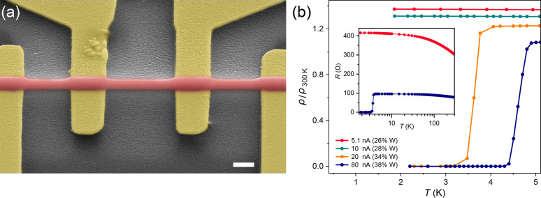
(a) False-color scanning electron micrograph of a W–C wire (red), contacted with gold electrodes (yellow). The scale bar corresponds to 500 nm. (b) Normalized resistivity of W–C wires deposited by beam currents ranging between 5.1 and 80 nA. Each wire is deposited with 25 ms dwell time and 60% beam overlap. Resistance is measured using a 10 μA dc bias. Legends show the W concentrations (atomic percentages) estimated from EDX analysis. The inset compares the temperature-dependent resistance of the wires made by 5.1 and 80 nA beams.
We use 20 nA as the standard beam current for fabricating our junctions. This corresponds to a beam spot diameter of around 60 nm in our instrument. For this beam current, the optimal values of dwell time and pitch (step size) are found to be 25 ms and around 1 nm, respectively (note that the optimal values differ from those used for writing the wires of Figure 1). These parameters result in wires with a typical Tc of 4.7 K (see Figure 2b) and a room temperature resistivity of ρ ≈ 270 μΩ cm (ρ(300 K)/ρ(10 K) ≈ 0.85). Increasing the beam current to 80 nA can raise the Tc even further to 5.7 K (see Supporting Information). Such high currents, however, can lead to electrostatic charging effects and larger beam spots, which limit our control over device fabrication. The bottom line here is that EBID can provide superconducting W–C with a Tc that is comparable to those written by IBID using Ga+ ions.4−9
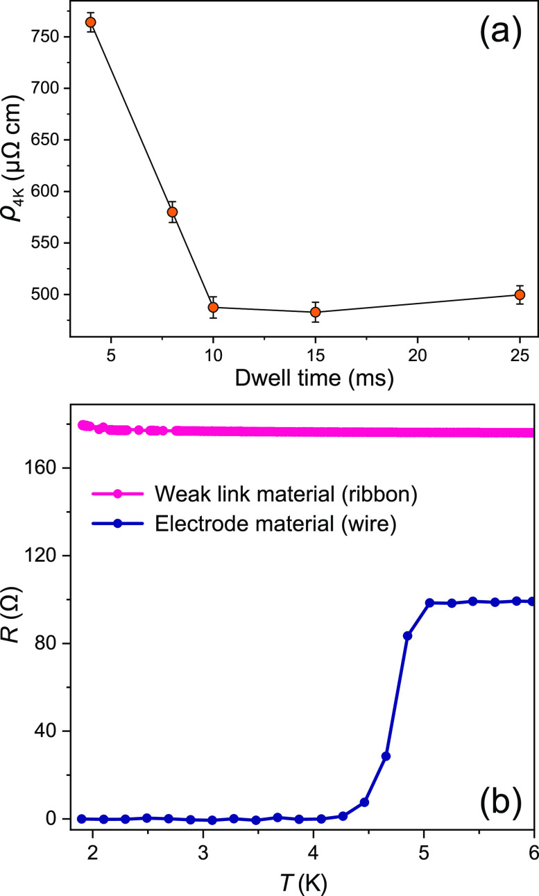
(a) Resistivity of W–C ribbons (prototypes for weak link) at 4 K as a function of EBID dwell time. (b) Temperature-dependent resistance of a superconducting W–C electrode wire, made using optimal parameters (blue), and a non-superconducting W–C ribbon (pink), both measured using a 10 μA bias. The structures are deposited using a 20 nA beam current and are of similar dimensions. The wire (written in line scan mode with 25 ms dwell time) and the ribbon (written by raster scans with 4 ms dwell time) represent the transport characteristics of the superconducting electrodes and the non-superconducting proximity weak links used in the final junctions, respectively.
Weak Link Material
A Josephson junction requires a weak link that segregates the superconducting condensates of the electrodes, while also coupling their wave functions to yield a single-valued current-phase relation. Naturally, the superconducting order parameter needs to be locally suppressed at the weak link. We achieve this by connecting superconducting W–C wires via a separate W–C segment with lower metallicity, where superconductivity is suppressed. Above, we demonstrated that beam current has a substantial influence over the electrical characteristics of the W–C and can be tuned to obtain both superconducting and normal metal components with which to fabricate junctions. However, writing the weak link with a different beam current than the electrodes would not be practical due to the additional refocusing necessary when switching the aperture of a SEM. A more effective approach is to utilize the dwell time, i.e., the time the electron beam spends per pixel. Longer dwell times are known to enhance the metallicity by increasing the number of electron scattering events per precursor molecule, which leads to a more efficient carbonyl (CO) desorption.18,19 We examine this using rectangular W–C ribbons, which serve as prototypes for the weak link materials used in the final EBID junctions. The ribbons are deposited by raster scanning a 20 nA beam in steps of 23 nm over a 200 nm wide rectangle. Depending on the dwell time, the number of raster scans used for each ribbon is adjusted to maintain the total applied dose constant. Figure 2a shows the resistivity of the W–C ribbons at 4 K (ρ4K), plotted as a function of dwell time. The error bars correspond to the uncertainty involved in estimating the cross-sectional area of the ribbons.
We observe a significant reduction of resistivity by increasing the dwell time to 10 ms, where it appears to approach a lower limit. The results indicate that there is a range of dwell times which can be used for tuning weak link conductivity. In Figure 2b, we compare the transport behavior of a high-quality W–C wire, written using 25 ms dwell time (line scan in 1 nm steps), together with a W–C ribbon of the same length, deposited with 4 ms dwell time (raster scan with 23 nm step size). The former is used in the superconducting electrodes of our EBID junctions, whereas the latter is representative of the weak link material that couples the electrodes together.
Josephson Junctions
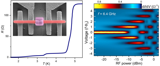
Figure 3a shows a typical EBID Josephson junction. The junctions are prepared by first depositing the superconducting electrodes, which are around 160 nm apart (Figure 3a, inset). The electrode wires are subsequently connected by a weak link, a 0.5 μm sized W–C square, deposited with a shorter dwell time, using a raster scan. It is worth mentioning that we found no electrical contribution from the delocalized (halo) deposits, which are known to form around EBID structures. Without the weak link material to connect the electrodes, no current could be measured across the 160 nm gap. Figure 3b–d shows the basic transport properties for three different Josephson junctions made in this way. JJ1 and JJ2 are printed using the same parameters for the weak link, with a 4 ms dwell time. This dwell time is increased to 10 ms for JJ3 in order to enhance its metallicity. Figure 3b shows the temperature-dependent resistance of the three junctions, measured with a 10 μA bias. It should be noted that JJ1 is deposited on a different substrate, where the distance between the gold voltage contacts is around three times larger, resulting in a higher normal-state resistance. The R(T) of each junction exhibits two main transitions: one at higher temperatures (typically around 4.5 K), representing the superconducting transition of the electrodes, and a broader one at noticeably lower temperatures (see the inset), which corresponds to the emergence of proximity-induced correlations in the weak link. Below the second transition, EBID junctions develop a clear Ic, as demonstrated by the current–voltage (I–V) measurements in Figure 3c,d. Furthermore, we find no hysteresis in the I–V characteristics.
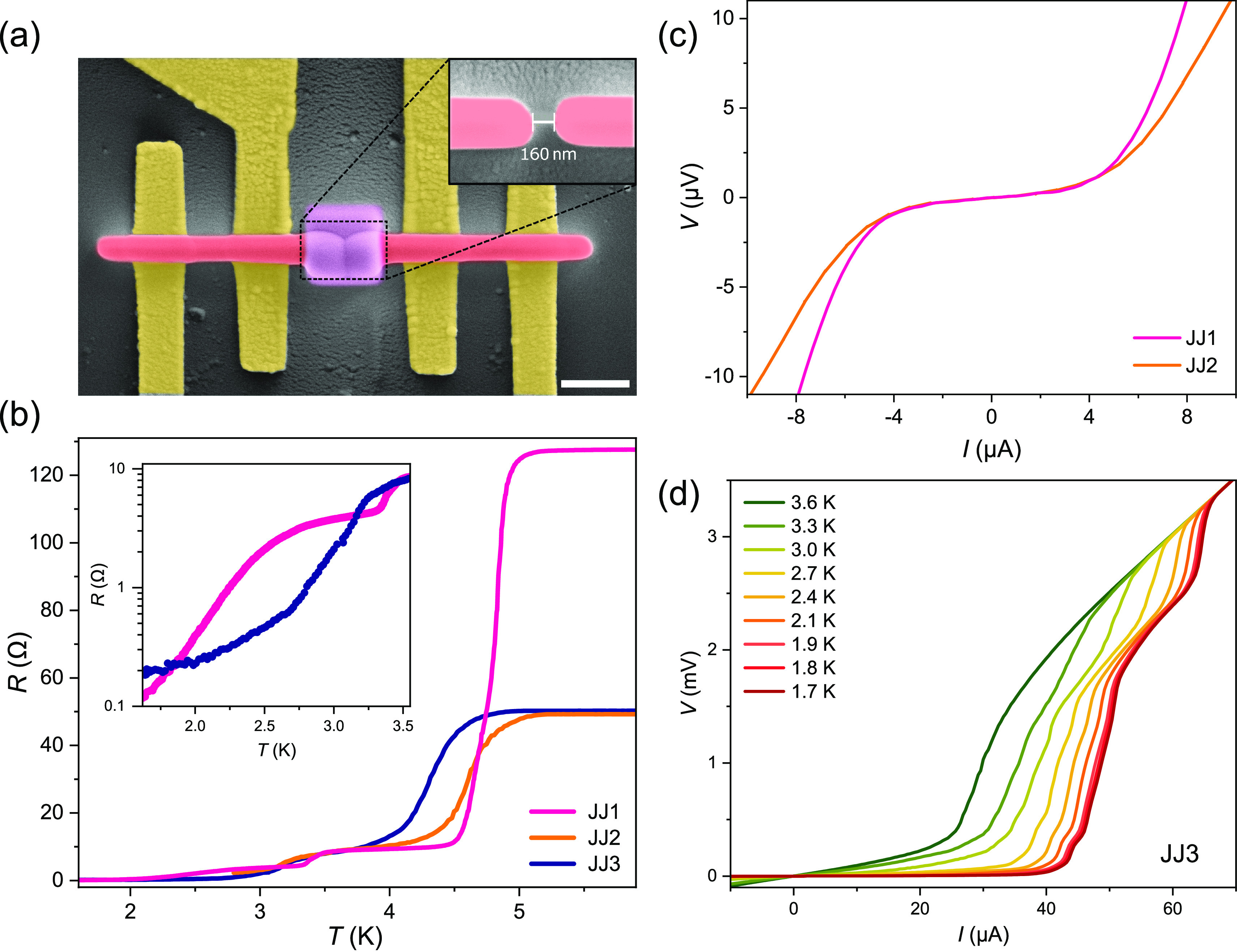
(a) False-color micrograph of an EBID Josephson junction. A W–C weak link (purple) connects two superconducting W–C electrodes (red), printed on gold contacts (yellow). Scale bar represents 1 μm. Inset image, taken prior to the deposition of the weak link material, shows the 160 nm gap that separates the superconducting electrodes and represents the effective length of the weak link. (b) Temperature-dependent resistance of three EBID junctions, measured with a 10 μA bias current. Inset shows the proximity-induced transition of JJ1 and JJ3 weak links, plotted on a logarithmic scale. (c) I–V characteristics of JJ1 and JJ2 weak links (both made with 4 ms dwell time), taken at 1.5 K. (d) I–V characteristics measured at different temperatures for JJ3 (weak link made using 10 ms dwell time).
Figure 3c shows that applying the same scanning parameters to deposit the weak links of JJ1 and JJ2 results in a matching Ic for both junctions. This is despite the fact that the junctions are fabricated on separate substrates and on different days. For junctions made with 4 ms dwell time, the typical IcRN product is between 10 and 14 μV. Here, RN corresponds to the normal-state resistance of the weak link and is determined by the value of dV/dI for I > Ic at T ≈ 1.5 K (when the weak link is fully proximized). The weak link of JJ3 was deposited with a higher dwell time (10 ms) compared to JJ1 and JJ2 (4 ms). Hence, due to the enhanced metallicity of its weak link, JJ3 yields a substantially higher Ic (see Figure 3d), corresponding to IcRN ≈ 50 μV.
It should be noted that, at T = 1.5 K, the base temperature of our cryostat, the junctions exhibit some finite resistance. For JJ3, this is 0.12 Ω, which is 10% of the normal-state resistance of the weak link, whereas JJ1 and JJ2 both have a resistance of around 0.11 Ω, which corresponds to 3–6% of their respective RN. The residual resistance can be seen as the slight slope in the I–V characteristics for I < Ic (see Figure 3c). This finite resistance may vanish by lowering the temperature or it may maintain a finite value due to some form of a phase slip process. While its exact origin is not clear at this stage, as demonstrated below, the resistance is not caused by a lack of coherent Josephson transport.
To unambiguously establish the Josephson transport in our EBID devices, we measured their Shapiro response to a radio frequency (RF) excitation. When external RF radiation couples to the junction dynamics by driving an additional RF supercurrent, it leads to the emergence of Shapiro steps in the I–V characteristics. These are discrete voltage steps that appear at V = nhf/2e = nf Φ0, where f is the microwave frequency, n is an integer, and Φ0 is the superconducting magnetic flux quantum. The Shapiro response of our junctions was verified by irradiating them with microwave frequencies from a nearby antenna (an open-ended coax, positioned a few millimeters above the sample) while measuring their I–V characteristics using a dc current bias. Figure 4 provides clear examples of the Shapiro response measured for 10 and 4 ms EBID junctions (JJ3 and JJ1, respectively). Figure 4a shows the Shapiro steps in the I–V curve of JJ3. In order to show the f Φ0 quantization of the steps in Figure 4a, the linear background, caused by the residual resistance at 1.5 K, has been subtracted from the I–V. The Shapiro response of JJ1 is shown by the differential resistance (dV/dI) curves in Figure 4b. For each junction, the steps occur at exactly integer multiples of f Φ0. The effect was reproduced for various microwave frequencies.
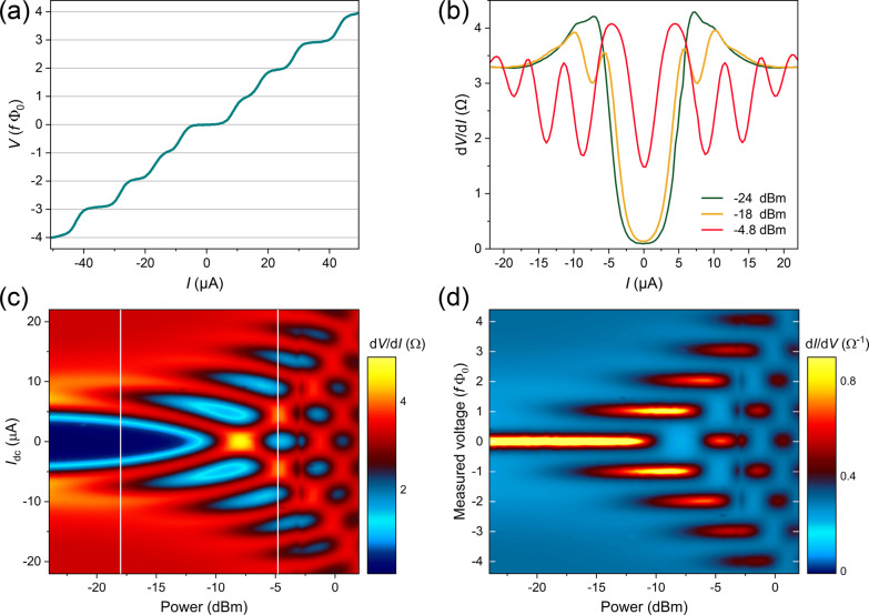
Shapiro response of junctions JJ1 and JJ3 to microwave irradiation of f = 6.4 GHz frequency. (a) I–V characteristic of JJ3, measured at 1.5 K. To emphasize the Shapiro steps, the voltage scale is normalized in units of f Φ0. The linear background, caused by the residual resistance of the device, has been subtracted from the I–V. (b) Differential resistance (dV/dI) of JJ1 at 1.64 K, measured for different RF powers. Shapiro steps manifest themselves as the “valleys” in the dV/dI, which emerge by increasing the power. (c,d) Evolution of the Shapiro response of JJ1 with RF power, shown as colormaps of dV/dI (c) and differential conductance dI/dV (d). White lines in (c) correspond to the measurements in (b). To demonstrate the quantized Shapiro response, the voltage in (d) is scaled in units of f Φ0.
We also explored the evolution of Shapiro steps with RF power. This was carried out by mapping the dV/dI as a function of RF power and dc current (swept from negative to positive bias). The results for JJ1 are presented as colormaps in Figure 4c,d in the form of differential resistance and differential conductance (dI/dV), respectively. To demonstrate the quantization of the Shapiro response more clearly, the measured voltage in Figure 4d is normalized in units of f Φ0. The power-dependent Shapiro response of JJ3 is included in the Supporting Information.
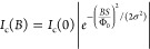
In addition to the Shapiro response, we use magnetic field-dependent measurements as an independent approach to verify the Josephson transport in our devices. The field-dependent critical current Ic(B) of a single Josephson junction is often associated with the well-known Fraunhofer diffraction pattern, in which Ic goes to zero when the magnetic flux applied to the junction is an integer multiple of Φ0. However, depending on their exact shape, dimensions, and material characteristics, Josephson junctions can exhibit widely different Ic(B) patterns. The elastic mean free path of W–C (l ≈ 0.3 nm)20,21 is much shorter than the superconducting coherence length (ξ ≈ 6 nm),22 which, in turn, is smaller than the length of the junction (L ≈ 160 nm), making the EBID junctions long and highly diffusive. It has been demonstrated that for long and diffusive junctions with narrow contacts, where the length and width of the weak link are comparable to each other, and also smaller than the penetration depth (λ = 1.05 × 10⁻³≈ 830 nm),23Ic(B) follows a Gaussian-like decay, given by
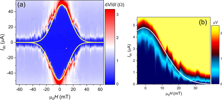
(a) Field-dependent dV/dI of JJ3 for positive and negative current bias, measured at 1.5 K by sweeping the out-of-plane magnetic field (from negative to positive) in 1 mT steps. (b) Field-dependent response of JJ1, obtained by I–V scans taken while sweeping the field (40 to −5 mT). The results in (a) and (b) are both fitted with the same Gaussian expression, as described by eq 1.
Lastly, we point out that the Josephson effect only occurs in structures with a well-defined weak link that can introducing a stable boundary between the condensates of the electrodes. Individual W–C wires exhibit no Shapiro response or a Gaussian-like Ic(B) pattern; they maintain a finite Ic, which gradually disappears as the field approaches the upper critical field of W–C, Hc2 ≈ 4 T. An inhomogeneous wire which still acts as a single condensate cannot yield a single-valued current-phase relation to support Josephson transport. An example of such a system is discussed in the Supporting Information.
Conclusion and Outlook
To summarize, we apply EBID to develop a fully additive direct-write approach to fabricating full proximity Josephson junctions inside an SEM, where both superconducting and normal metal components can be printed by regulating the parameters of the scanning electron beam. This principle is extended to provide a reliable means for tuning the critical current of the junctions. We also demonstrate that EBID can produce superconducting W–C, with Tc reaching as high as 5.7 K, which so far had only been reported for W–C structures made with IBID.
Given the widespread availability of electron microscopes, the EBID approach presented here provides an accessible and relatively inexpensive means to fabricate Josephson devices such as SQUIDs and single-photon detectors.26 The ability to directly print a Josephson junction on a given surface, without the use of energetic ions or wet processing, expands the current applications of superconducting electronics. This is particularly advantageous when dealing with nonplanar surfaces, mechanically fragile substrates (e.g., membranes, free-standing beams, and cantilevers) and systems that are vulnerable to chemical processing. Even more enticing is the capacity of EBID for 3D nanoprinting. With the advent of hybrid Monte Carlo–continuum simulations and computer-aided design programs, pioneered by Fowlkes et al.(27) and Huth and Keller,28 the field of 3D EBID has received a renewed boost in recent years. By implementing the recently developed computational approach to EBID, the growth of complex 3D structures can be simulated and optimized prior to the actual deposition.29 Combining such simulations with the EBID Josephson junctions presented here provides an exciting opportunity for realizing 3D-printed superconducting circuits and quantum networks.
Methods
Procedure for Printing a Josephson Junction
All junction devices are written using a 10 keV electron beam with 20 nA beam current, corresponding to a beam-spot diameter of around 60 nm in our instrument (Apreo SEM by Thermo Scientific with a gas injection system). The typical base pressure of the microscope chamber is about 2 × 10⁻⁶ mbar. Once the W(CO)6 precursor is injected, the pressure increases to around 2 × 10⁻⁵ mbar.
To print a Josephson junction, first, the superconducting electrodes are deposited onto a Si3N4-coated silicon substrate by scanning the beam in a straight line (i.e., the “line scan mode”), applying 25 ms dwell time and 1 nm pitch (step size). The wires are written in a single row, separated by a gap of 160 nm. Once the electrodes are formed, they are connected via a tungsten carbide weak link, deposited by raster scanning the beam over an area of approximately 0.5 × 0.5 μm2, using 23 nm step size. The dwell time used in writing the weak link is 4 ms for JJ1 and JJ2 and 10 ms for JJ3. To obtain transparent interfaces for efficient proximity, it is important to minimize the time interval between the formation of the electrodes and the deposition of the weak link.
Measurements
Transport measurements were performed in a variable-temperature cryostat, where sample temperature could be regulated between 300 and 1.5 K. At low temperatures, the temperature stability of the system was better than 1 mK. Resistance and current–voltage (I–V) characteristics were measured in a four-probe configuration, using a current-biased circuit and a nanovoltmeter or, alternatively, a lock-in amplifier (both setups produced the same results). The Shapiro response of the junctions was obtained by measuring their I–V characteristics while irradiating them with microwave frequencies from a nearby antenna. The procedure was repeated for multiple frequencies, including f = 6.4 GHz (shown in the article). In each case, the height of the voltage steps varied in accordance to f Φ0. Magnetotransport measurements were taken by sweeping the field in the out-of-plane direction.
Supporting Information Available
The Supporting Information is available free of charge at https://pubs.acs.org/doi/10.1021/acsnano.0c03656.
Additional details on the superconducting transition and normalized resistivity versus temperature graph of wires deposited with 80 nA; transport measurements and SEM image of an inhomogeneous wire; Shapiro response of device JJ3; a table containing the parameters used in the fabrication of the W–C wires and ribbons discussed in this work (PDF)
Notes
The authors declare no competing financial interest.
Acknowledgments
This work is part of Project No. 680-91-128, which is (partly) financed by the Dutch Research Council (NWO).